





Content last revised on September 10, 2026
Benchtop Waveform Tuning: Mitigating Stress via Bi-Directional DC-DC Buck-Boost Conversion on 2M120B150J-120
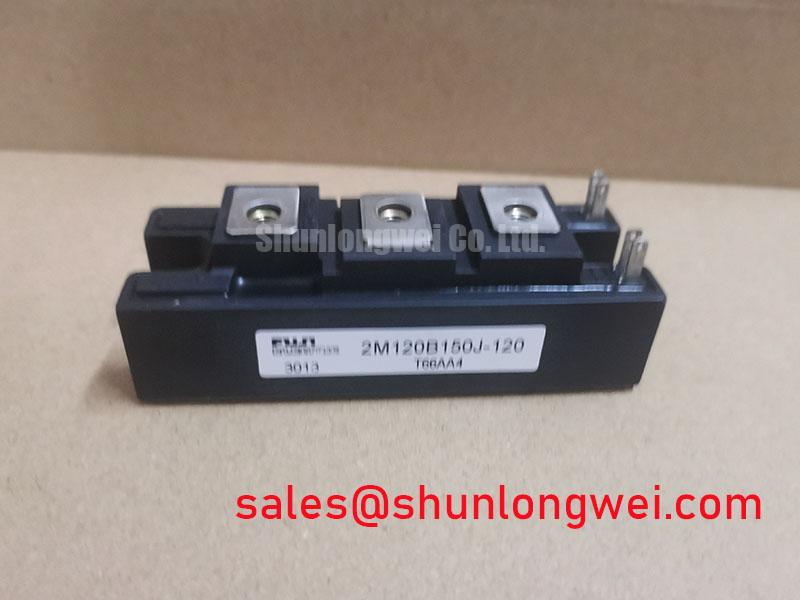
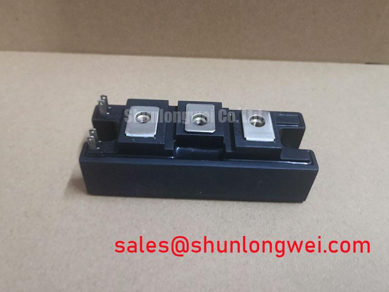
With the converter fully isolated and discharged, first verify that the installed module marking matches 2M120B150J-120, then inspect power terminals, mounting surfaces, and gate-drive connections for heat discoloration, looseness, contamination, or mechanical damage before applying any electrical test voltage.
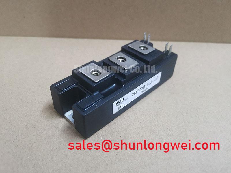
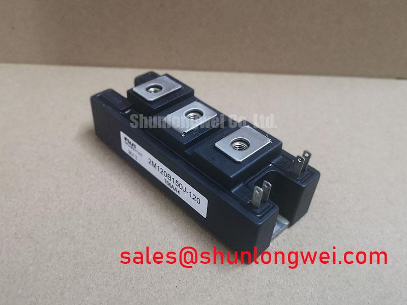
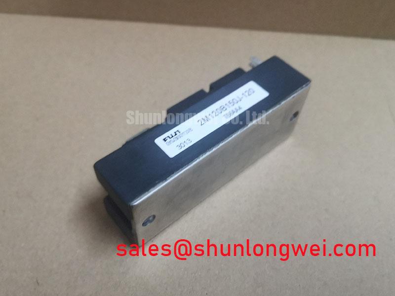
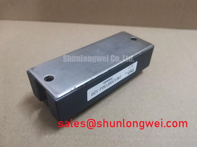
The Fuji Electric 2M120B150J-120 is a Fuji Power Module rated at 1200 V and 150 A according to the official product specification. These ratings establish the device identity and provide the starting electrical boundary for maintenance assessment, DC bus architecture review, and gate-drive verification. The system integrator should confirm the original equipment circuit topology, driver interface, cooling arrangement, and protection thresholds before installation.
| Parameter | Specified Value | Classification |
|---|---|---|
| Part number | 2M120B150J-120 | Official product identification |
| Manufacturer | Fuji Electric | Official product identification |
| Voltage rating | 1200 V | Official Specification |
| Current rating | 150 A | Official Specification |
| Product family | Fuji Power Module | Product family description |
In a bidirectional DC DC buck boost stage, the 2M120B150J-120 can be evaluated where battery-side energy and inverter-link energy move in both directions. Commercial string inverter and micro-grid energy storage platforms can expose the switching assembly to repeated charge and discharge transitions, especially when operating conditions change between battery support, load balancing, and DC-link regulation. The official 1200 V and 150 A ratings must be assessed against actual measured switching peaks rather than nominal bus conditions alone.
A practical bench procedure begins with isolated gate-drive confirmation, followed by low-energy commissioning and controlled waveform capture across the relevant switching nodes. Engineers should compare turn-on and turn-off behavior with the known-good phase or leg where available. Ringing, unexpected voltage overshoot, irregular collector current transitions, or inconsistent gate waveforms may indicate a layout, drive-return, snubber, DC-link, or connection issue. They should be investigated through measurement rather than attributed to one component without verification.
💡 Pro Tip: Keep the DC-link busbar path compact and symmetrical around the commutation loop, then validate turn-off peak voltage margins with double-pulse testing under the actual system conditions.
Design Consideration: minimize parasitic loop inductance between the DC-link capacitors, module power terminals, and commutating path to suppress inductive overshoot during switching. The final layout, busbar geometry, capacitor placement, and damping network must be determined by the system engineer through waveform validation against the operating DC-link voltage and load current.
For repair planning, confirm that the replacement module has the required electrical ratings, terminal arrangement, mechanical interface, and driver compatibility. The 3MBI50SX-120-02 can be reviewed as a related Fuji Electric power-module reference, but it requires independent verification of current capability, topology, pinout, thermal path, and operating conditions before any substitution decision.
Benchtop Waveform Tuning: Mitigating Stress via Thermal Paste Degradation Prevention and Mounting Practices on 2M120B150J-120
Before mounting the 2M120B150J-120, clean the heatsink contact plane and module base contact area using an approved process that leaves no fibers, hardened compound, debris, or raised contamination. Thermal interface compound should be applied as a thin and continuous layer. Design Consideration: an interface thickness in the general range of 50 to 100 µm is commonly used for power-module mounting, but the correct quantity and process must be validated against the mechanical requirements of the cooling assembly.
Use a sequential screw-tightening pattern so mounting pressure develops progressively across the baseplate. This helps reduce the risk of localized stress and uneven thermal contact caused by a tilted mounting sequence. The applicable screw size, torque, washer arrangement, heatsink flatness, and baseplate curvature accommodation should be confirmed from the original equipment documentation and module mechanical drawing. Do not treat general mounting practice as an official torque specification for this particular module.
During troubleshooting, compare thermal behavior across comparable converter sections using the same measurement method and load condition. A temperature difference can arise from interface quality, airflow, liquid-cooling flow, heatsink flatness, switching loss variation, current imbalance, sensor placement, or control behavior. Rework the thermal interface only after identifying whether the abnormal condition follows the module, the cooling surface, or the operating channel.
Complementary gate commands also require review when a module is reinstalled. Design Consideration: dead-time and gate interlock behavior should prevent simultaneous conduction of opposing switches during commutation. The required timing margin is system-determined and should be verified at the gates and power terminals under representative voltage, current, temperature, and transient conditions. A gate-drive controller that appears correct at no load can behave differently during high-current switching because return-path voltage movement affects the effective gate-emitter signal.
Benchtop Waveform Tuning: Mitigating Stress via Negative Gate Bias vs Active Miller Clamping on 2M120B150J-120
Fast voltage transitions at a switching node can capacitively couple into the gate circuit and raise the gate-emitter voltage of an inactive device. This Miller-related effect can become significant when the gate loop has excessive impedance, the emitter return is poorly referenced, or the driver protection arrangement is not matched to the measured transient behavior. The 2M120B150J-120 should therefore be evaluated with probes connected close to the relevant gate-drive reference points, using an appropriate measurement method that does not create a misleading loop.
Negative gate bias and active Miller clamp functions are alternative control approaches that may be present in a system gate driver. They are not official device parameters of this Fuji Electric module. Design Consideration: select and validate the gate-drive strategy according to observed dv dt behavior, driver isolation capability, gate-loop layout, and the voltage limits specified in the original module documentation. The system engineer should validate that an inactive device remains securely off during the highest expected commutation stress.
When unwanted turn-on is suspected, inspect the driver supply stability, gate resistor integrity, clamp path continuity, driver output symmetry, gate-return routing, and DC-link decoupling placement. Oscilloscope traces should be compared with a verified channel wherever possible. Replacing a gate resistor or adding a clamp without confirming the actual transient can shift switching loss, oscillation, and protection timing in ways that are not visible during static checks.
For broader topology context, the article Resonant Topologies in Home Appliances provides useful reference material on switching-path behavior and converter topology distinctions. Although the application context differs, the measurement discipline of observing commutation current paths and switching-node voltage behavior remains relevant to power-stage fault isolation.
Assembly Integrity & Layout Architecture: Implementing Galvanic Gate Drive Isolation, Reinforced for 2M120B150J-120
Verify the gate-drive isolation barrier as part of the complete converter assembly, not as an assumed property of the power module. Reinforced isolation capability, insulation coordination, creepage, clearance, and common-mode transient immunity are determined by the selected driver, isolation components, PCB construction, enclosure, and system voltage environment. These characteristics require review against the applicable equipment standards and original design documentation.
Maintain physical separation between high-energy power conductors and sensitive gate-drive traces. Design Consideration: route gate and return conductors as a tightly coupled pair, avoid sharing high-current return paths with the control reference, and preserve the intended creepage and clearance distances around high-voltage terminals. The layout should be checked after assembly because bent conductors, excess solder, loose hardware, or altered cable routing can reduce intended spacing.
In commercial string inverters and micro-grid energy storage equipment, communication and monitoring boards may be electrically close to the power stage. Industrial communication references such as Industrial Ethernet can help frame the need to control noise coupling between switching hardware and networked control nodes. Display and HMI integration should also be treated as a separate system-level interface concern; industrial display references such as Truly Semiconductors Industrial Display Modules are useful when reviewing display-node integration requirements.
Before returning the equipment to service, inspect terminal fastening, cooling contact, gate-drive polarity, control interlock behavior, protective-device coordination, and insulation spacing. Semiconductor fuses and other upstream protective elements should be evaluated as a coordinated system function, including their clearing behavior and energy-withstand relationship to the converter architecture. No field-life, fault-energy, EMC-compliance, isolation-reliability, or safety-certification claim should be inferred from the module’s 1200 V and 150 A official ratings alone.