Content last revised on September 10, 2026
Multi-Module Parallel Current Sharing & Positive Tempco Dynamic Balancing
Operating high-capacity commercial string inverters and micro-grid energy storage systems (BESS) pushes power semiconductors through demanding load-cycling profiles. The 7MBR150XNE120-50 from Fuji Electric is rated at VCES = 1200.0V and continuous collector current IC = 150.0A (Official Datasheet Specification). In centralized battery-coupling stages or high-power AC output bridges where multiple modules run in parallel, managing current distribution between individual dies is critical to prevent localized thermal runaway.
At the silicon level, the module leverages trench-gate field-stop technology characterized by a positive temperature coefficient of saturation voltage (VCE(sat)) across its primary operating window. When junction temperature rises within one channel during peak current delivery, its VCE(sat) naturally shifts upward, redirecting excess current into parallel channels with lower relative thermal loading. While this physical characteristic provides robust steady-state thermal balance, dynamic current sharing during turn-on and turn-off transients depends entirely on symmetric PCB layout and parasitic loop inductance control.
When paralleling converter stages, asymmetric gate-loop impedance produces switching time skews between units. A variance of just a few nanohenries in auxiliary gate traces forces the faster-switching module to absorb the full turn-on current spike. To guarantee dynamic balance, field service teams must verify that all parallel gate and auxiliary emitter lines feature identical trace lengths, identical gate damping resistors (with initial sizing calculated per gate charge requirements), and paired twisted-lead routing. For engineers evaluating system redesigns or legacy hardware retrofits, comparing this architecture against modular half-bridge configurations like the 2MBI150-060 allows for precise optimization of loop inductance versus assembly complexity.
Optimizing Heatsink Contact Pressure and Surface Roughness for Minimum R_th(c-s)
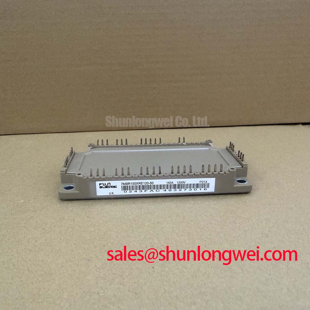
Thermal impedance between the module baseplate and the extruded cold plate directly defines device longevity under continuous high C-rate cycling. The 7MBR150XNE120-50 integrates a 7-pack topology encompassing an inverter bridge, a dedicated brake chopper, and an integrated thermistor. Extracting heat across this expansive copper baseplate demands strict compliance with mechanical flatness, thermal interface material (TIM) application, and mounting fastener torque profiles.
| Mechanical Parameter | Specification / Requirement | Classification |
|---|---|---|
| Heatsink Surface Flatness | ≤ 50 μm per 100 mm span | Design Consideration |
| Heatsink Surface Roughness (Rz) | ≤ 10 μm | Design Consideration |
| Target TIM Wet Thickness | 50 μm – 100 μm (Screen-printed) | Design Consideration |
| Mounting Bolt Size & Sequence | M5 / Cross-pattern (Initial hand-tight, then final torque) | Design Consideration |
| Rated Mounting Torque | 2.5 – 3.5 N·m | Typical Starting Point |
⚠️ Field Alert: Never apply thermal grease with a continuous bead in the baseplate center or use an uncalibrated electric drill during heatsink mounting. Uneven spread patterns trap air voids beneath the isolated DCB substrates, drastically increasing case-to-sink thermal resistance Rth(c-s). Always use a precision metal squeegee or 50-mesh screen stencil to lay down a uniform 50 to 100 μm film. When tightening baseplate screws, follow a diagonal cross pattern: pre-tighten all screws to approximately 1.0 N·m, wait 10 minutes for grease relaxation across the micro-grooves, and then apply final torque between 2.5 and 3.5 N·m.
During field service audits of overheated or tripped inverter racks, technicians should clean mating surfaces with isopropyl alcohol, inspect the cold-plate surface for burrs around threaded holes, and verify the integrity of external connections using standard verification workflows detailed in the Field Engineer’s Handbook.
Auxiliary Emitter Return Trace Separation for Rapid dv/dt Transients
High-speed switching of 150A inductive currents at 1200V creates severe voltage rate-of-change (dv/dt) transients across the converter phase nodes. In compact PIM assemblies, high di/dt passing through the main power emitter creates an induced voltage across parasitic lead inductances. If the gate driver references the main power ground instead of the dedicated Kelvin emitter terminal, this transient voltage directly modulates the gate-to-emitter potential.
Parasitic feedback induced on the gate path can drop VGE below the threshold during conduction—forcing the IGBT into its active desaturation zone—or trigger spurious turn-on events leading to catastrophic shoot-through. To isolate gate control from the main output power path, the 7MBR150XNE120-50 provides independent auxiliary emitter terminals. Driver circuits must route the gate return signal strictly to this auxiliary pin, ensuring the high-current load return path remains completely separated on the PCB layout.
For auxiliary systems and lower-power intermediate conversion blocks, engineers often review companion modular drivers and complementary switches such as the 6MBI10S-120 to maintain standard layout practices across system boards. Comprehensive topology guidelines and packaging details for integrated industrial solutions can be reviewed via Fuji Electric Power Semiconductor & IPM Modules and official documentation for the Fuji Electric PIM (Power Integrated Module) 7-Pack platform.
DC-DC Converter Interleaving and Ripple Current Cancellation for Lithium Banks
In utility-scale and commercial micro-grid storage setups, the interface between lithium battery racks and the high-voltage DC link requires bi-directional buck-boost or interleaved multi-phase topologies. Operating under alternating charging and heavy C-rate discharging conditions exposes the IGBT dies to continuous junction temperature cycles (ΔTj), accelerating bond-wire stress and solder joint fatigue.
The integrated brake chopper section within the 7MBR150XNE120-50 functions as a versatile switching arm for energy dump circuits, auxiliary DC-DC boost stages, or active overvoltage clamping during grid disconnect events. Interleaving two or more converter phases driven by complementary pulse-width modulation (PWM) effectively multiplies the ripple frequency on the battery DC bus while dividing the current magnitude per branch. This ripple cancellation significantly reduces ESR-related ohmic heating in the battery storage bank and lowers RMS stress across the DC-link capacitor bank.
When conducting diagnostic sweeps on non-responsive or fault-tripped inverter modules, follow these practical multimeter validation steps before reconnecting the DC bus:
- Collector-to-Emitter Junction Check: Set the digital multimeter (DMM) to Diode Test mode. Measure across all upper and lower IGBT switches (Collector to Emitter). A forward drop across the anti-parallel freewheeling diode typically reads between 0.3V and 0.6V, while the reverse reading must indicate infinite resistance (open-circuit OL).
- Gate-to-Emitter Insulation Verification: Measure resistance between Gate and Auxiliary Emitter pins on all arms using the high-megohm resistance range. A healthy gate oxide must read open circuit (> 50 MΩ); any reading below 1 MΩ indicates dielectric degradation or electrostatic gate punch-through.
- NTC Thermistor Characterization: Measure the integrated thermistor pins at ambient temperature. Cross-reference the measured resistance against the official nominal 5 kΩ or 10 kΩ rating curve to rule out internal substrate cracking.
- Brake Chopper Diode Continuity: Verify forward and reverse drop on the dedicated dynamic brake diode terminals to confirm dynamic braking circuits are protected against back-EMF spikes.