




Content last revised on June 28, 2026
MG100H2CL1 Datasheet, Specs & Analysis: 600V 100A Dual IGBT Module
An Engineering-Focused Overview
Your Guide to This Proven Half-Bridge Power Module
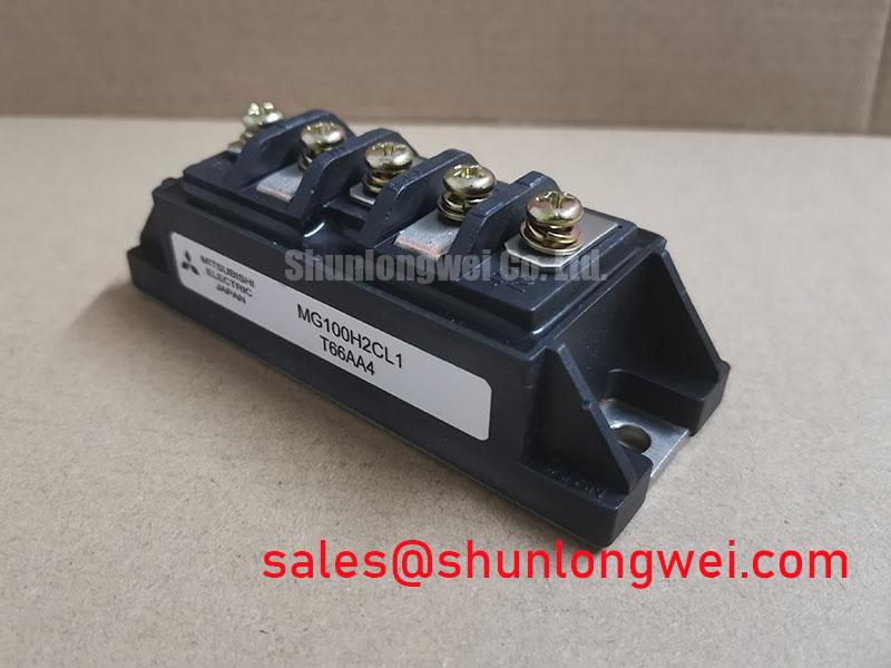
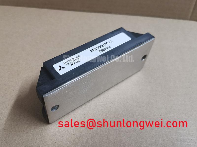
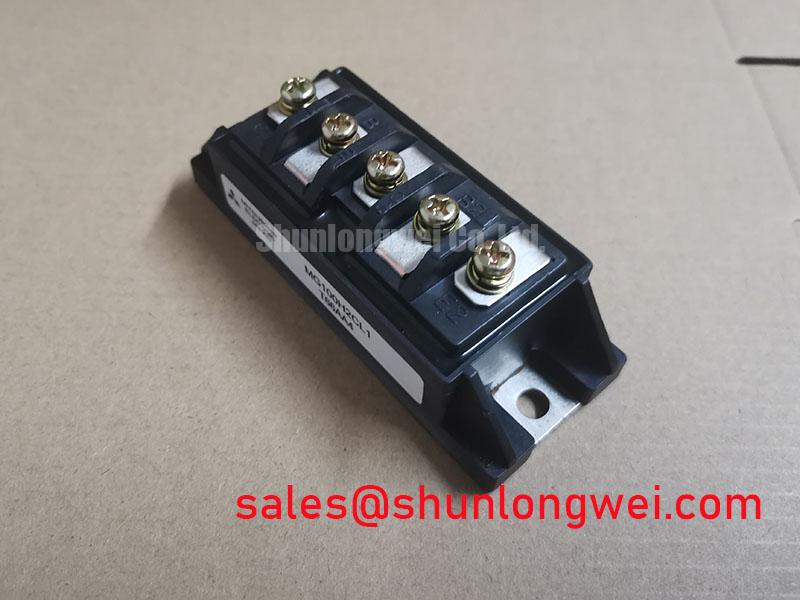
The Toshiba MG100H2CL1 is a robust 600V dual IGBT module engineered for efficient and reliable power switching in industrial motor control and Switch-Mode Power Supply (SMPS) applications. It delivers a balanced performance profile with key specifications of 600V | 100A | VCE(sat) 2.7V max. This integration provides two primary engineering benefits: a simplified half-bridge design and performance optimized for moderate switching frequencies. Its well-defined VCE(sat) and thermal characteristics are critical for accurately calculating and managing power losses in PWM-driven systems, directly addressing core design challenges. For 240V AC motor drives up to 20kW requiring a proven and integrated power stage, the MG100H2CL1 provides a reliable building block.
Application Scenarios & Value
Optimizing Performance in Industrial Drives and Power Conversion Systems
The MG100H2CL1 is engineered for medium-power applications where operational reliability and straightforward design are paramount. Its most common use case is in the inverter stage of a Variable Frequency Drive (VFD) or a high-power SMPS.
Consider the design of a VFD for a 15kW AC induction motor. A primary engineering challenge is managing thermal dissipation to ensure long-term reliability without specifying an oversized, costly heatsink. The MG100H2CL1's dual IGBT configuration directly simplifies the physical layout of the inverter leg, reducing component count and parasitic inductance compared to using discrete IGBTs. More importantly, its clearly specified maximum collector-emitter saturation voltage (VCE(sat)) of 2.7V allows engineers to perform a precise worst-case analysis of conduction losses for a given Pulse Width Modulation (PWM) strategy. This predictability is fundamental to designing a cost-effective and adequate thermal solution that guarantees performance under load. For systems operating on higher voltage lines or demanding greater current capacity, the related QM150DY-24 offers a 1200V, 150A rating.
Key Parameter Overview
A Specification Breakdown for Loss Calculation and Thermal Design
The technical specifications of the MG100H2CL1 are foundational for any system design. The following table highlights the parameters most critical for performance and reliability assessments. Understanding these values is the first step in successful circuit modeling and thermal management.
| Parameter | Symbol | Conditions | Value |
| Collector-Emitter Voltage | VCES | VGE = 0V | 600V |
| Gate-Emitter Voltage | VGES | ±20V | |
| Collector Current (DC) | IC | Tc = 80°C | 100A |
| Collector Current (1ms Pulse) | ICP | Tc = 80°C | 200A |
| Collector Power Dissipation | PC | Tc = 25°C | 480W |
| Collector-Emitter Saturation Voltage | VCE(sat) | IC = 100A, VGE = 15V | 2.7V (Max) |
| Thermal Resistance (IGBT) | Rth(j-c) | Junction to Case | 0.4 °C/W |
| Thermal Resistance (FWD) | Rth(j-c) | Junction to Case | 0.8 °C/W |
| Turn-On Time | ton | IC = 100A | 1.0 µs (Typ) |
| Turn-Off Time | toff | IC = 100A | 1.5 µs (Typ) |
| Diode Forward Voltage | VF | IF = 100A | 2.5V (Max) |
Technical Deep Dive
Analyzing Conduction vs. Switching Losses for System Efficiency
An IGBT's efficiency is determined by the sum of its conduction and switching losses. The MG100H2CL1, with its typical VCE(sat) of 2.3V, is optimized for applications where conduction losses are a significant portion of the total loss budget. This is common in industrial motor drives and welding power supplies that operate at moderate switching frequencies, typically in the 5 kHz to 15 kHz range.
The trade-off between these two loss types can be compared to choosing a delivery vehicle. A large, powerful truck (analogous to a low VCE(sat) IGBT) is highly efficient for long, continuous highway hauls (low-frequency operation with long on-times), but it's inefficient to constantly start and stop in city traffic (high switching losses). Conversely, a small, nimble van (higher VCE(sat) IGBT) excels at frequent stops and starts (high-frequency operation) but is less efficient on the highway. The MG100H2CL1 acts as the reliable workhorse truck, providing excellent performance for the sustained power delivery cycles found in many industrial applications. Engineers must use the Eon and Eoff energy loss curves in the datasheet to balance these factors and find the optimal operating frequency for their specific load profile.
Frequently Asked Questions (FAQ)
Engineering Questions on the MG100H2CL1
What is the primary advantage of the dual (half-bridge) configuration in the MG100H2CL1?
The main advantage is system integration. What is the primary benefit of its dual configuration? Reduced layout complexity and component count. By housing two IGBTs and two free-wheeling diodes in a single, thermally-optimized package, it simplifies the design of an inverter phase leg, reduces PCB space, and minimizes stray inductance between the high-side and low-side switches.
How does the maximum VCE(sat) of 2.7V impact the thermal design for a motor control application?
The VCE(sat) is the voltage drop across the IGBT when it is fully on. This value is essential for calculating the worst-case conduction power loss (Power Loss = VCE(sat) × IC × Duty Cycle). Using the 2.7V maximum rating ensures the thermal design, including heatsink selection, has enough margin to keep the IGBT junction temperature within its safe operating limits even under the most demanding load and temperature conditions.
Is a negative gate voltage required for turning off the MG100H2CL1?
Yes, the datasheet's switching characteristics are specified with a gate-emitter voltage (VGE) of +15V/-10V. Using a negative voltage for turn-off provides a stronger buffer against noise and parasitic turn-on induced by the Miller effect (dV/dt), ensuring more reliable and robust switching performance, especially in noisy industrial environments.
Strategic Role in Industrial Power Systems
A Foundation for Reliable and Predictable Power Design
While the power electronics industry continually evolves with new semiconductor technologies, modules like the MG100H2CL1 serve a critical role. Their value is rooted in proven field reliability, extensive documentation, and a performance profile that is thoroughly understood and optimized for the core applications of industrial power conversion. For design engineers developing systems where long-term operational stability, design predictability, and a streamlined assembly process are key objectives, this module provides a solid and dependable foundation.