
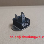
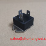
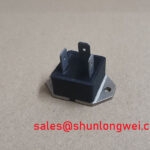

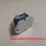
Content last revised on October 9, 2026
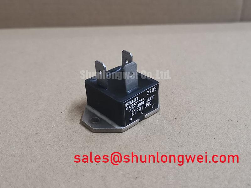
Transient Dynamics and Electrical Design for ETF81-050
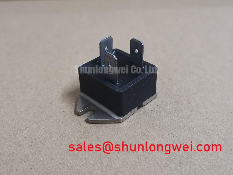
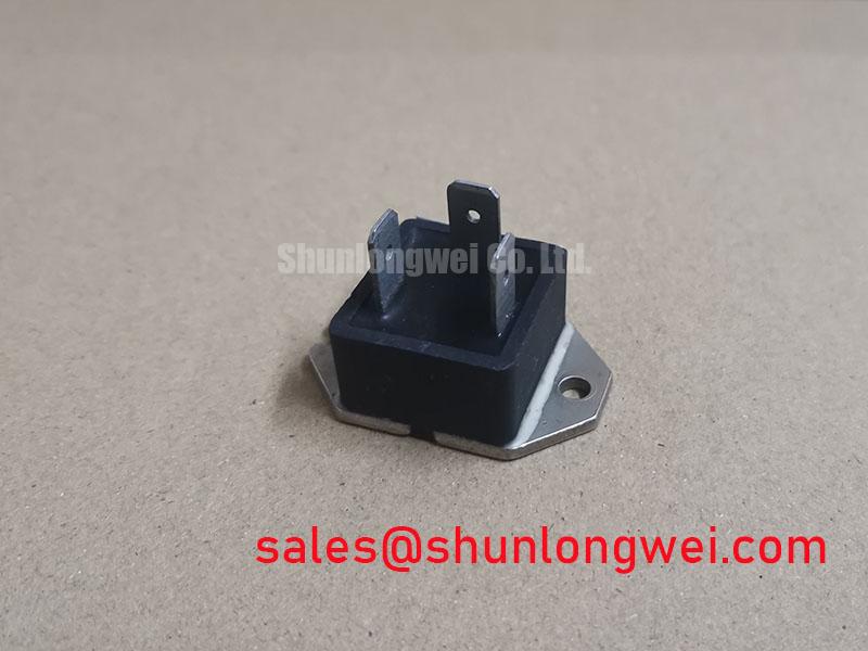
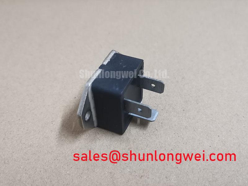
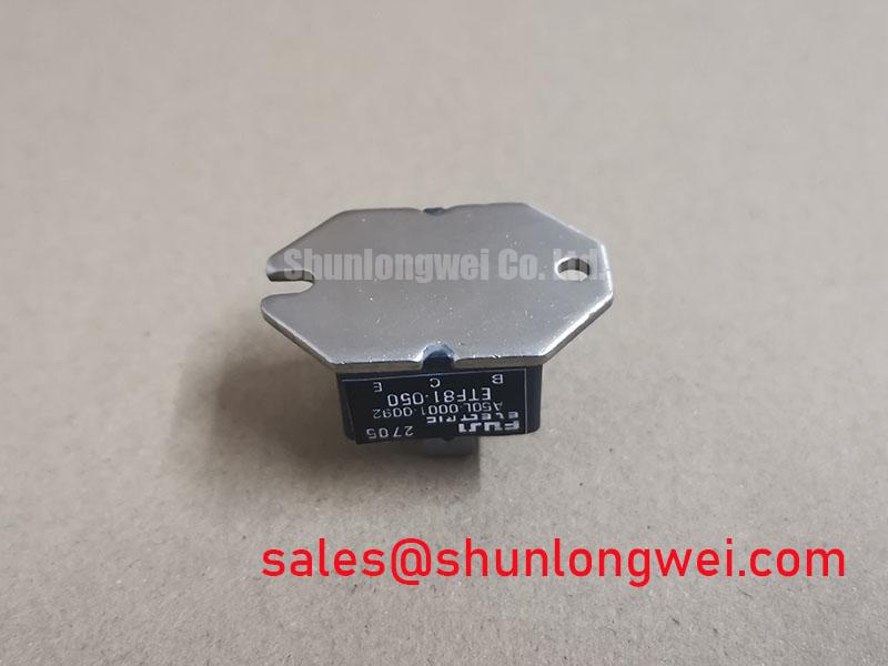
| Product | ETF81-050 |
|---|---|
| Manufacturer | Fuji Electric |
| Category | IGBT Module |
| Rated Voltage | 600.0 V Official Specification |
| Rated Current | 50.0 A Official Specification |
| Package | Module Official Specification |
Measure the installed busbar geometry and capture the turn off voltage at the module terminals before changing gate drive or snubber values. The Fuji Electric ETF81-050 is specified as a 600.0 V, 50.0 A IGBT module, but those ratings do not describe the complete switching environment created by a servo drive, inverter, or regenerative motor actuator. The practical task is to control the voltage overshoot produced by commutation inductance while keeping the switching loop compact, symmetrical, and thermally serviceable.
During turn off, the additional voltage is governed by the interaction between stray inductance and current slew rate. In engineering terms, the peak voltage rises as the DC link voltage is combined with the inductive contribution associated with Lσ and di/dt. This relationship is useful during waveform review, but it is not a substitute for a measured double pulse or operating-load test. Probe placement is especially important: a long ground lead can display an artificial spike, while a probe connected across a remote capacitor may hide the stress appearing directly at the module terminals.
A planar laminated busbar is a Design Consideration when the switching loop shows excessive ringing. Place the outgoing and return conductors close together, keep the commutation path short, and avoid routing the gate return beside a high-current collector or emitter path. Symmetrical geometry helps distribute current and reduces the magnetic loop area. A sub-25 nH value should be treated as a system design target, not as an ETF81-050 manufacturer specification. The final geometry should be verified by measurement under the intended DC-link voltage, load current, and gate resistance.
Use the local DC-link film capacitor as close to the power terminals as the mechanical assembly allows. A remote bulk capacitor can support low-frequency energy storage while contributing little to the fastest switching edge. When a snubber is evaluated, connect it across the switching path it is intended to control rather than at a convenient but electrically distant point. The capacitor, resistor, and physical connection must be selected together because a low-inductance capacitor with a long lead arrangement can still produce poor transient control.
Field waveform work should compare the same switching event at light load, rated operating load, and regenerative operation. Look for the combination of overshoot, ringing frequency, duty-cycle dependence, and temperature sensitivity. A change that reduces the first voltage peak but increases ringing duration may transfer stress into another part of the circuit. Designers should verify the peak voltage margin against the DC-link voltage and the module’s rated voltage during representative switching tests.
Gate-drive symmetry also matters in a bridge leg. Keep the gate loop separate from the high-current power loop, use a controlled return path, and verify that the driver reference remains stable during the highest di/dt event. Gate resistor selection is system-dependent; a typical starting point may be used during bench tuning, but the final value should be established from switching loss, overshoot, dead time, and thermal measurements rather than copied from an unrelated module.
For a replacement assessment, compare the electrical topology and terminal arrangement before comparing only voltage and current numbers. The 2MBI400TB-060-02 can be reviewed as a separate same-voltage-class reference, but it should not be treated as an automatic substitute for the ETF81-050. Confirm the original drive’s terminal mapping, gate-drive polarity, mechanical interface, and thermal assembly before any interchange decision.
Benchtop Waveform Tuning and Baseplate Isolation Testing
Start the isolation audit with the module completely disconnected from the gate driver, snubber network, motor cable, and DC-link assembly. A terminal-to-baseplate insulation test is a Design Consideration for incoming inspection and service diagnosis; the stated criterion of at least 500 MΩ at 2.5 kV DC should be treated as a test-plan value only when it is supported by the applicable component documentation and the insulation tester’s procedure. It is not one of the three confirmed listing specifications for this part.
Clean, dry contact surfaces are essential before applying an insulation test. Dust, flux residue, condensation, and conductive contamination can create a surface leakage path that does not represent an internal insulation condition. Record the test configuration, test duration, ambient conditions, and the exact points connected to the instrument. After the test, discharge the module and connected capacitance through an approved method before touching the terminals or reconnecting the driver.
The baseplate check should be performed separately from the semiconductor junction checks. A resistance measurement between power terminals can be affected by internal diode paths, parallel circuit connections, or the measuring instrument’s test current. Use the wiring diagram of the original assembly to isolate the module, then compare the readings across corresponding terminals. A result that differs from a known-good unit should trigger a controlled repeat with clean contacts and correct polarity, not an immediate conclusion about a particular internal failure.
Where the module construction documentation identifies an insulated ceramic substrate, inspect the surrounding assembly for mechanical distortion, contamination, and evidence of uneven clamping. Do not infer substrate damage from a single resistance value. Check whether the result changes after the external snubber and motor cable are removed, then inspect the mounting plane and interface material. The purpose is to separate module insulation behavior from leakage introduced by the wider power stage.
Phase-angle conduction and line-frequency ripple belong to the upstream converter and control strategy, not to the ETF81-050 rating label. If the module is used in a controlled rectifier or servo power stage, observe how the firing angle changes the DC-link ripple and the current waveform. Gate pulses should arrive with stable amplitude and timing at the module terminals, and the driver supply should remain within the limits specified for the actual driver circuit. The IGBT module should not be assigned a gate voltage range that has not been confirmed from its applicable datasheet.
RC snubber tuning should follow the measured ringing event. Place the current probe and voltage probe so that their bandwidth and loop area do not distort the result. Adjust one network variable at a time, then review switching loss and device temperature as well as peak voltage. An RC network that appears effective at one load point may produce unnecessary dissipation during continuous operation. The correct balance is established by the system designer from measured transient energy, switching frequency, and thermal capability.
💡 Bench Tip: Use ESD protection, record a cold-state reference from a known-good installation, and discharge the module safely before reconnecting any cable.
When the ETF81-050 is evaluated in a precision stepper or BLDC motor servo actuator, capture the phase-current waveform during acceleration, steady motion, and deceleration. A distorted waveform can result from current-sensor scaling, control-loop timing, DC-link ripple, gate-drive behavior, or power-device stress. Review the complete signal path instead of assigning the symptom to the IGBT module alone.
Regenerative DC-Bus Voltage Surge Dissipation for ETF81-050
Measure the DC-bus rise during the actual deceleration profile before selecting a braking IGBT or ballast resistor. A servo actuator returns kinetic energy to the DC link when the motor slows, and the resulting voltage rise depends on motor inertia, speed, commanded deceleration, bus capacitance, braking duty, and the energy path available in the drive. The ETF81-050 carries a 600.0 V rated voltage and 50.0 A rated current according to the supplied official specification, but braking-network sizing remains a system-level calculation.
The braking branch should be evaluated as a coordinated switch, resistor, sensing circuit, and thermal assembly. The external or internal braking IGBT must be selected against peak current, pulse duration, switching loss, repetitive duty, and the actual gate-drive arrangement. The ballast resistor must absorb the required braking energy without exceeding its pulse rating or creating an unsafe enclosure temperature. Use the motor manufacturer’s inertia and speed data together with measured bus voltage to establish the energy envelope.
A braking resistor that is suitable for a short emergency stop may be unsuitable for repeated indexing. Review the duty cycle as a time history rather than a single peak event. In a precision motion actuator, frequent short decelerations can create substantial average heating even when each individual pulse appears modest. The thermal path from resistor to enclosure and the airflow around the assembly should be included in the evaluation.
Coordinate the braking threshold with the DC-link capacitor, surge absorber, and control firmware. MOV protection can assist with transient suppression, but its clamping behavior, energy rating, leakage, and repetitive duty must be matched to the bus voltage and fault-clearing strategy. An MOV is not a replacement for a correctly sized regenerative braking path. The same principle applies to RC networks: they can reduce high-frequency overshoot while the braking branch handles slower energy return.
During troubleshooting, place the voltage probe directly across the DC link and use a current probe in the braking branch. Compare the event with the braking command, fault signal, and gate pulse. If the bus rises while the braking command is absent, inspect sensing polarity, controller timing, wiring continuity, and gate-drive enable logic. If the command is present but the branch current is not, inspect the driver supply, gate path, device connection, and resistor circuit. These observations narrow the fault area without assuming a single failed component.
Check the mechanical installation after electrical verification. The baseplate or heatsink interface must remain flat and clean, and the clamping arrangement must distribute pressure evenly across the module. A spring-loaded or disc-spring arrangement can help maintain contact force through thermal cycling, but its calibration is an engineering and assembly responsibility. Follow the applicable Fuji Electric mechanical instructions for the actual module construction rather than applying a generic torque or pressure value.
For a power topology that includes a rectifier or auxiliary front end, the 2MBI200U2A-060-50 may be reviewed as a separate device reference. Its presence in a related power stage does not establish compatibility with the ETF81-050. Confirm the bus voltage, current path, control method, isolation requirements, and thermal arrangement for each position in the circuit.
Use the IGBT Design & Integration guide when reviewing gate-drive layout, thermal transfer, and protection coordination across the complete converter. For additional manufacturer context on integrated power semiconductor approaches, consult the Fuji Electric RC-IGBT Modules resource; it should be read as product-family information rather than as a specification for ETF81-050.
Before returning a repaired drive to service, repeat the isolation test, confirm the gate and power terminal mapping, capture the DC-link waveform during the most demanding deceleration, and compare the measured thermal response with the approved operating procedure for the equipment.