Content last revised on September 26, 2026
Fuji Electric 2MBI200VA-060-50: Key Specifications
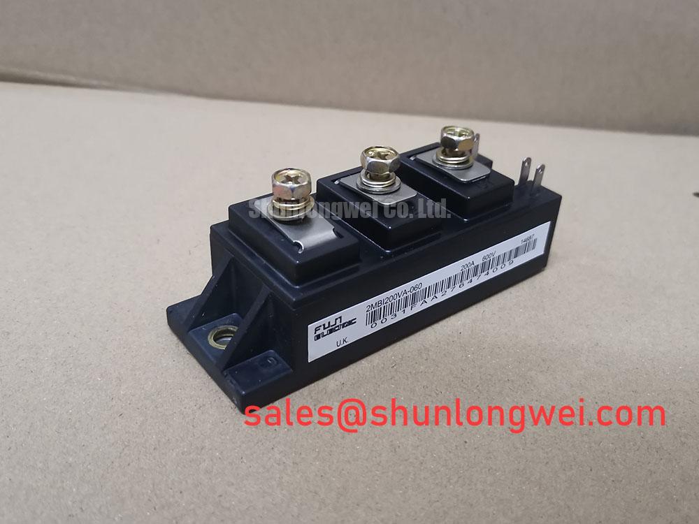
Before energizing a replacement position, verify the nameplate rating, inspect the baseplate and terminals, and measure the installed circuit against the known-good phase leg with power fully isolated. The Fuji Electric 2MBI200VA-060-50 is a 600 V, 200 A IGBT module intended for evaluation in high-power switching equipment, including industrial inverter welders and medium-frequency induction heating power supplies.
| Parameter | Official Specification |
|---|---|
| Collector-emitter voltage | 600 V VCES |
| Continuous collector current | 200 A at TC = 80°C |
| Repetitive peak collector current | 400 A ICP |
| Junction temperature | −40°C to +150°C |
| Isolation voltage | AC 2500 V for 1 minute |
| Collector-emitter saturation voltage | 1.85 V at VGE = 15 V and IC = 200 A |
| Gate-emitter threshold voltage | 4.5 V to 8.5 V |
| Input capacitance | 19.6 nF CIES |
| Turn-on time | 0.40 μs |
| Turn-off time | 0.45 μs |
2MBI200VA-060-50 Circuit Protection and Reliability: Thermal Interface Control
Start thermal work by cleaning the heatsink contact surface and checking the module baseplate for contamination, burrs, local distortion, or uneven contact marks. The official continuous collector-current rating of 200 A at TC = 80°C depends on the thermal conditions of the complete assembly, not on the module alone. A clogged fan path, aged thermal interface material, or loose mounting hardware can therefore change the real operating margin even when the electrical load has not changed.
Thermal interface material should be applied as a controlled, continuous film rather than as isolated beads. A commonly used engineering starting range for power-module mounting is approximately 50 to 100 μm, but the final process must be validated against the selected compound, surface finish, flatness, and assembly method. Excess compound can increase thermal resistance, while insufficient coverage can leave air voids beneath the baseplate. Designers should inspect witness patterns after trial assembly and confirm contact uniformity with temperature measurements during a controlled load test.
Mounting screws should be tightened in a gradual diagonal sequence so that the baseplate is seated without introducing excessive local stress. The correct torque is an assembly-process value determined by the module drawing, screw size, washer arrangement, heatsink material, and plant work instruction; it should not be assumed from the electrical rating. After commissioning, compare the temperatures of equivalent phase legs and check whether one position shows a persistent rise under the same current waveform.
Maintain practical clearance around the power terminals, gate wiring, and heatsink surfaces so that conductive debris, condensation, or cable movement cannot create an unintended path. In inverter welders and induction heating supplies, inspect the cooling path during planned maintenance and check for dust accumulation near the inlet, fan, and heatsink fins. ⚠️ Maintenance Note: Monitor contact temperature trends and verify the cooling airflow after cleaning or replacing the thermal interface material.
For a neutral comparison point during an approved hardware evaluation, engineers may review the electrical and mechanical documentation for 2MBI300U4H-120-50. Any substitution requires confirmation of circuit topology, gate-drive requirements, mounting geometry, isolation, current conditions, and protection coordination rather than a comparison of voltage and current numbers alone.
Field Diagnostics and Commissioning: Active Miller Clamp Evaluation
During commissioning, inspect the gate-emitter waveform at the module terminals rather than relying only on the driver-board test point. The 19.6 nF CIES official input-capacitance value indicates that the driver and wiring must be evaluated as a switching network. Gate-loop inductance, common-emitter inductance, driver impedance, and the opposing switch voltage can all influence the observed waveform.
High dv/dt at the complementary device can couple current through the Miller capacitance and raise the gate voltage of the device that should remain off. An active Miller clamp is a Design Consideration for reducing this unwanted gate movement by providing a low-impedance discharge path after the driver command reaches the off state. Its timing, current capability, isolation arrangement, and compatibility with the selected gate driver must be verified by the system designer. The negative gate-bias range suggested for some high-speed topologies must also be confirmed against the actual module and driver documentation; it should not be treated as an official rating for this product without a supporting datasheet.
Use an oscilloscope with suitable differential probes to examine turn-on, turn-off, gate overshoot, collector-emitter voltage, and current commutation together. The official switching times are 0.40 μs turn-on and 0.45 μs turn-off, but measured system behavior will vary with gate resistance, DC-link conditions, load current, temperature, stray inductance, and the test circuit. A discrepancy between phase legs may indicate wiring imbalance, driver timing variation, or a power-loop issue; verify each condition against a known-good waveform before changing the gate network.
Reverse recovery from a freewheeling diode can increase commutation current and produce voltage ringing in the power loop. Snubber selection, busbar arrangement, diode behavior, and switching speed should therefore be considered together. Designers should minimize parasitic loop inductance, then verify peak voltage against the 600 V VCES boundary during switching tests. EMC performance belongs to the assembled equipment and its installation; the module itself should not be represented as independently certified to an equipment-level emissions standard. The Fuji Electric V-Series IGBT Application Manual provides useful manufacturer application context for gate drive and switching evaluation.
Preventing Spurious Faults: Transient Thermal Response and Pulse Loading
A high-current pulse should be evaluated through the complete thermal path rather than through the continuous-current figure alone. The official 400 A repetitive peak collector current rating identifies a specified current capability, but it does not replace the pulse duration, duty cycle, switching state, cooling condition, and protection limits defined for the equipment. A maintenance team investigating intermittent overtemperature or protection trips should capture collector current, DC-link voltage, case temperature, ambient temperature, and pulse repetition at the same time.
Transient thermal impedance is commonly represented by a multi-stage RC network so that short pulses and longer load intervals can be assessed separately. This is an Engineering Calculation method, not an additional factory rating. The calculation should use the manufacturer’s applicable thermal data, the measured case temperature, and the actual pulse profile. When such data are unavailable, avoid assigning a numerical junction-temperature margin from the nameplate alone. Instead, use controlled load testing and compare the measured case-temperature response with the approved thermal model.
For battery charging and discharging converters, repeated bidirectional current flow can create thermal cycling even when the average power appears acceptable. Inspect the heatsink attachment, interface material condition, fan response, and phase-current sharing after representative charge and discharge sequences. In an induction heating supply, the work-coil control pattern can produce a different pulse distribution from a steady inverter load, so the thermal model should reflect the real switching sequence rather than a simplified constant-current assumption.
When a protection event occurs, record whether it followed a long high-load interval, a rapid current transition, a regenerative event, or a cooling interruption. These observations help separate thermal accumulation from electrical overshoot without assuming a single cause. Check the module’s gate-emitter behavior, collector-emitter waveform, thermal sensor location, and protection threshold as separate evidence streams. The junction operating range specified for this module is −40°C to +150°C; equipment-level control limits must be set and validated by the system designer using the complete thermal path.
For broader background on IGBT switching physics, thermal networks, and application verification, consult The Ultimate IGBT Knowledge Base. It should supplement, not replace, the applicable Fuji Electric documentation and the measured behavior of the finished assembly.
Preventing Spurious Faults: Overvoltage Protection During Fast Switching
Begin a DC-link overvoltage investigation by recording the bus voltage, braking command, switching-node voltage, motor or load speed, and fault timing on the same time base. In regenerative braking, stored mechanical energy can return to the DC link faster than the main load can consume it. A braking chopper and resistor may be used in the system, but their voltage threshold, pulse capability, cooling, duty cycle, and protective coordination must be selected from the equipment energy calculation rather than inferred from the 600 V module rating.
The braking resistor must absorb the expected braking energy without exceeding its thermal and pulse limits, while the braking IGBT must withstand the resulting current and switching stress. These are system-level design values. Designers should verify the worst-case deceleration profile, DC-link capacitance, resistor temperature, chopper waveform, and overvoltage-trip response under controlled testing. A resistor that appears adequate during a short bench test may behave differently during repeated production cycles or restricted-airflow operation.
Fast switching can expose stray-inductance voltage spikes that are not visible on a slow meter. Use a properly rated differential probe and a short measurement loop, then compare the switching-node waveform with the gate command and current trace. If ringing appears near a protection threshold, evaluate busbar geometry, snubber placement, gate resistance, diode recovery, and braking-control timing as a coordinated network. Do not lower the protection threshold or increase switching speed without confirming the resulting voltage and thermal margins.
The module’s official isolation specification is AC 2500 V for 1 minute, but insulation coordination for the finished inverter or welding supply also depends on creepage, clearance, pollution level, enclosure condition, and wiring layout. In installations exposed to humidity or condensation, inspect terminals and insulating surfaces during scheduled shutdowns and verify that the cooling system does not draw contaminated moisture across high-voltage areas. Fuji Electric semiconductor resources, including its power semiconductor reference material, can be used alongside the specific module documentation when reviewing switching-device application constraints.