Content last revised on October 3, 2026
7MBR50U2A060 Fuji Electric 600V 50A PIM Power Module
| Parameter | Official Specification |
| Manufacturer | Fuji Electric |
| Model | 7MBR50U2A060 |
| Rated voltage | 600.0 V |
| Rated current | 50.0 A |
| Package | Module |
| Product category | PIM, intelligent or power module category |
Begin a replacement inspection by isolating the equipment, recording the original wiring, and checking the nameplate boundary of 600.0 V and 50.0 A before removing the installed power module. The 7MBR50U2A060 is a Fuji Electric module intended for evaluation in power conversion assemblies where the circuit, cooling system, gate drive, protection network, and mechanical interface are all verified against the original equipment design.
The published product data identifies this device as a Module with a rated voltage of 600.0 V and a rated current of 50.0 A. These are official product parameters supplied for identification and initial engineering screening. They do not, by themselves, define the permissible switching frequency, overload duration, junction temperature, short circuit withstand, thermal resistance, insulation rating, or safe operating area. Those values should be confirmed from the applicable Fuji Electric documentation and the original equipment service data. The Fuji Electric power semiconductor portal is a suitable reference point for manufacturer documentation.
For light industrial automation and multi-joint robotic articulator repairs, the first compatibility check should compare the DC link, phase output arrangement, gate interface, auxiliary terminals, mounting pattern, cooling contact, and protection feedback with the installed unit. Do not infer an interchangeable pinout from the same current class or package description. A procurement review should also retain photographs of the terminal markings and the original busbar orientation so that the replacement can be electrically and mechanically validated before energization.
Preventing Spurious Faults: Thermal Paste Degradation Prevention and Mounting Guidelines for 7MBR50U2A060
A clean thermal interface is the first practical control when installing the 7MBR50U2A060. Remove the old thermal interface material from the heatsink and module contact surfaces using a method approved for the equipment, then inspect the base contact area for scratches, raised edges, contamination, or visible distortion. The goal is continuous thermal contact without trapped air pockets. A thermal compound layer in the 50 to 100 µm range may be used as a general engineering consideration when it agrees with the module manufacturer’s mounting instructions and the selected compound’s application data; it is not an official rating of this model.
Baseplate flatness and heatsink condition matter because uneven contact can create local thermal concentration even when the module feels mechanically secure. Apply the compound uniformly rather than using a large central deposit that can leave uncovered regions after clamping. Excess compound can also migrate toward terminals and insulation surfaces. The system engineer should verify the selected thermal interface material for temperature range, electrical behavior, pump out resistance, and compatibility with the equipment’s service environment.
Use the original mounting hardware where its condition and specification are confirmed. Tighten the fasteners progressively in a diagonal or otherwise balanced sequence so that the module base settles evenly onto the heatsink. The correct torque is determined by the manufacturer’s mechanical documentation, fastener size, washer arrangement, and heatsink design. Do not treat a general M5 installation value as a guaranteed parameter for this product. After mounting, inspect the terminal height, busbar alignment, and any mechanical stress transferred to the module terminals.
Field Alert: Disconnect the DC link and auxiliary supplies, confirm an electrically safe state, and wait for verified discharge before touching module terminals or inserting control connectors.
If a replacement installation develops intermittent overtemperature or protection events, compare heatsink temperature at equivalent load, inspect the contact imprint after controlled disassembly, and check whether the cooling fan, duct, or thermal sensor is operating as expected. A fault that appears after warm-up may involve thermal contact, switching stress, current imbalance, or protection timing rather than the thermal compound alone.
In a robotic axis, keep power conductors physically separated from low level feedback and gate control wiring where the equipment layout permits. Minimize the area of the high current commutation loop to reduce induced voltage during switching. Clearance and creepage requirements remain system dependent and should be checked against the applicable working voltage, pollution environment, insulation system, and safety standard.
7MBR50U2A060 Thermal Electrical Optimization: Isolated DC DC Power Supply Sizing for Practical Tuning
The isolated gate supply should be evaluated as part of the complete switching circuit rather than selected from output voltage alone. Confirm the required gate voltage, source and sink current, startup behavior, undervoltage lockout, isolation rating, insulation construction, and common mode transient immunity from the gate driver and module documentation. A requirement such as reinforced isolation above 5 kV or a CMTI capability above 100 kV per microsecond can be relevant to a particular system, but these figures must be verified against the actual converter and driver datasheets rather than assigned to the 7MBR50U2A060 without a manufacturer source.
During bench commissioning, observe the gate to emitter waveform directly at the module terminals with suitable differential measurement equipment. A waveform that looks clean at the driver board can show ringing or a shifted reference at the power module because of connector inductance, emitter coupling, or an extended return path. The engineering objective is to preserve the intended gate signal while limiting false turn on during the opposite device’s transition. The final gate resistance, damping network, dead time, and drive supply arrangement are system determined and should be tuned using switching measurements.
Protection coordination also deserves a complete circuit review. A high speed semiconductor fuse should be selected only after comparing its clearing behavior with the converter’s prospective fault current, bus energy, wiring inductance, and the module’s documented short circuit or surge capability. Fuse I²t coordination is an engineering calculation based on the fuse data and system fault profile; the 50.0 A rating of the module is not a substitute for that calculation. Verify that the fault clearing path does not create a destructive overvoltage at the module terminals.
For a robotic articulator drive, inspect the isolated supply during acceleration, deceleration, regenerative events, and repeated direction changes. These operating points can expose control supply dips or common mode disturbances that are not visible during a steady state motor test. If the gate waveform changes with motor cable position or switching current, compare measurements at the driver output and at the module terminals, then review the isolation barrier, return path, shielding, and connector arrangement.
The device is not independently certified for complete equipment EMC compliance. The final assembly must be assessed as a system, including the motor cable, enclosure, grounding, filter network, switching pattern, and control electronics.
7MBR50U2A060 Operational Boundaries: Evaluating Differential Gate Source Loop Routing to Switching Limits
Route the gate signal and its return as a closely coupled differential loop from the driver to the relevant module terminals. Keep this loop away from the main commutation path and avoid sharing the gate return with high current emitter conductors. The purpose is to prevent voltage developed by common emitter inductance from appearing as an unintended gate signal. When an auxiliary or sensing emitter terminal is provided by the verified module documentation, its connection should be treated separately from the high current power return; do not assume terminal functions without checking the actual pin definition.
Oscillation during turn off can result from the interaction of gate impedance, driver output impedance, parasitic inductance, device capacitances, and measurement setup. A practical investigation begins with a short measurement connection at the module, followed by comparison of the turn on and turn off waveforms at different load currents. The engineer should examine gate voltage, collector or switch node behavior, and the driver supply at the same event. Any damping adjustment is a typical starting point for bench tuning, not a fixed 7MBR50U2A060 specification.
Keep the power loop symmetrical where the circuit topology allows it. Busbar placement, capacitor location, phase conductor geometry, and return path directly influence switching overshoot. The peak voltage should be verified against the system DC link and the documented device limits during double pulse or equivalent switching tests. Do not calculate an acceptable margin from the 600.0 V rating alone because the relevant transient, temperature, current, and switching conditions must be included.
For topology selection and fault interpretation in appliance or compact inverter arrangements, the discussion of Resonant Topologies in Home Appliances provides useful system context. It should be used as an application reference rather than as a substitute for the Fuji Electric data applicable to this module.
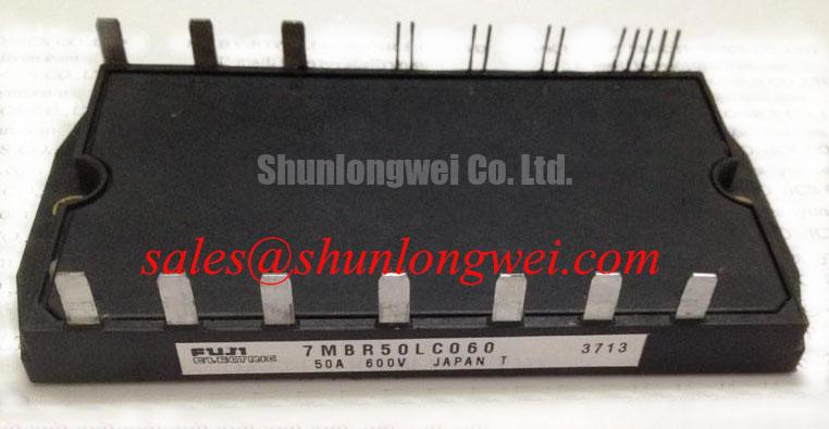
If the original assembly uses a related Fuji Electric power stage, engineers may compare its documented electrical and mechanical requirements with the neutral reference product 7MBR50LC060. This is a comparison exercise only; interchangeability must be established from verified terminal definitions, ratings, thermal data, and the equipment schematic.
7MBR50U2A060 Circuit Protection and Reliability: Calibrating Dynamic Power Loss Dissipation and Multi Resistance Thermal Networks
Thermal evaluation should combine conduction loss, switching loss, case temperature, cooling performance, and the actual load profile. The 50.0 A rating identifies the product’s stated current class, but it does not determine allowable current under every switching frequency, duty cycle, ambient condition, or heatsink arrangement. The design engineer should obtain the relevant loss curves and transient thermal impedance data from the applicable manufacturer documentation before calculating a peak junction temperature.
For pulsed overload analysis, a multi resistance and capacitance thermal model can represent how heat moves from the semiconductor junction to the case and then into the heatsink. In practical terms, the engineer applies the time varying loss profile to the documented transient thermal impedance, adds the measured or validated case temperature, and checks the resulting peak junction temperature against the applicable limit. This is an engineering calculation, not a field life guarantee. A short overload can produce a different thermal response from the same average power applied continuously.
Record the switching waveform and load current during the most demanding motion profile of the robotic axis. Repeated acceleration, braking, and holding periods should be assessed separately because conduction and switching losses may dominate at different points. If measured case temperature appears acceptable while electrical failures continue, inspect turn off overshoot, gate disturbance, current sharing, clamp action, and local busbar heating rather than relying on case temperature as the only diagnostic.
A MOV may form part of a coordinated overvoltage network, but its voltage rating, energy capability, clamping behavior, aging characteristics, and placement must match the DC link and fault environment. The MOV should be evaluated together with the DC link capacitor, semiconductor fuse, snubber, wiring inductance, and control shutdown path. It should not be presented as a universal solution for switching overshoot. Verify the protected node with an appropriately rated differential probe during the relevant transient event.
The gate oxide reliability discussion in Time-Dependent Dielectric Breakdown of Gate Oxides helps explain why repeated electrical overstress deserves attention, but it does not provide a product-specific lifetime prediction for this Fuji Electric model. Any lifetime, FIT rate, insulation reliability, or environmental qualification statement requires a traceable manufacturer or standards-based source.
Within the wider drive chain, engineers may also review another IGBT power stage represented by 6MBI100L-060. Its suitability depends on the complete power circuit, DC link, braking, control, and protection design. When replacing the 7MBR50U2A060, verify the original schematic, terminal sequence, thermal interface, gate drive behavior, and measured switching margins before returning the equipment to service.