Content last revised on September 10, 2026
7MBR35SB120-01 Operational Boundaries: Evaluating Optocoupler vs Digital Coreless Transformer Limits
Before connecting a replacement module, verify the drive nameplate and inspect the disconnected power stage for heat sink contamination, degraded thermal interface material, loose terminals, moisture traces, and damaged busbar insulation. The 7MBR35SB120-01 from Fuji Electric is a power module with an official 1200 V VCES rating, intended for inverter and braking functions within a controlled industrial drive assembly.
| Official Datasheet Specification | Value | Condition |
|---|---|---|
| Collector Emitter Voltage, VCES | 1200 V | Official rating |
| Inverter Collector Current, IC | 35 A | TC = 80°C |
| Brake Chopper Collector Current, IC | 25 A | TC = 80°C |
| Collector Emitter Saturation Voltage, VCE(sat) | 2.2 V typical, 2.7 V maximum | IC = 35 A, VGE = 15 V, Tj = 25°C |
| Inverter Power Dissipation, PC | 240 W | One device |
| Isolation Voltage, Viso | AC 2500 V for 1 minute | Official rating |
The module’s AC 2500 V for 1 minute isolation rating is an official module specification, but it does not define the required isolation rating, clearance, creepage distance, or common mode transient immunity of the complete gate drive board. Those properties must be verified at the system level from the converter DC link, installation category, insulation coordination plan, and gate driver documentation.
For a motion actuator inverter, investigate unexpected gate activity with the power stage disabled first. Compare the gate command at the controller output, isolation barrier output, and module gate terminal. A gate pulse appearing only after the isolation stage can indicate coupling through the driver supply, return path, control cable, or PCB layout. Design Consideration: keep high energy switching conductors physically separated from gate command traces and ensure the gate return follows a controlled, short path to reduce unwanted induced voltage.
Optocoupler based drivers and digital coreless transformer drivers use different internal isolation methods, so a direct substitution should not be assumed. The maintenance team should confirm driver supply sequencing, fault output polarity, desaturation or overcurrent protection behavior, and the controller’s permitted propagation delay before changing a drive board. Fuji Electric’s power semiconductor portal provides broader product family context, while the original equipment documentation remains the authority for the installed drive.
Transient Dynamics & Electrical Design: Sizing Braking Resistors and Chopper Transistor on 7MBR35SB120-01
The braking chopper section is officially rated at 25 A at TC = 80°C. During motor deceleration, regenerative energy raises the DC link voltage until the drive control activates a braking path. The resistor value, pulse energy capability, enclosure temperature, duty cycle, and chopper control threshold are system determined; they cannot be selected from the module current rating alone.
When a servo axis reports DC bus overvoltage during deceleration, verify the brake resistor connection, resistance against the machine documentation, thermal cutout circuit, and command waveform to the chopper gate. A resistor with damaged wiring or poor terminal contact may prevent energy dissipation, but controller configuration, excess inertia, and a restricted deceleration profile also require review. The inverter current rating remains 35 A at TC = 80°C, so braking and inverter current paths should be evaluated separately.
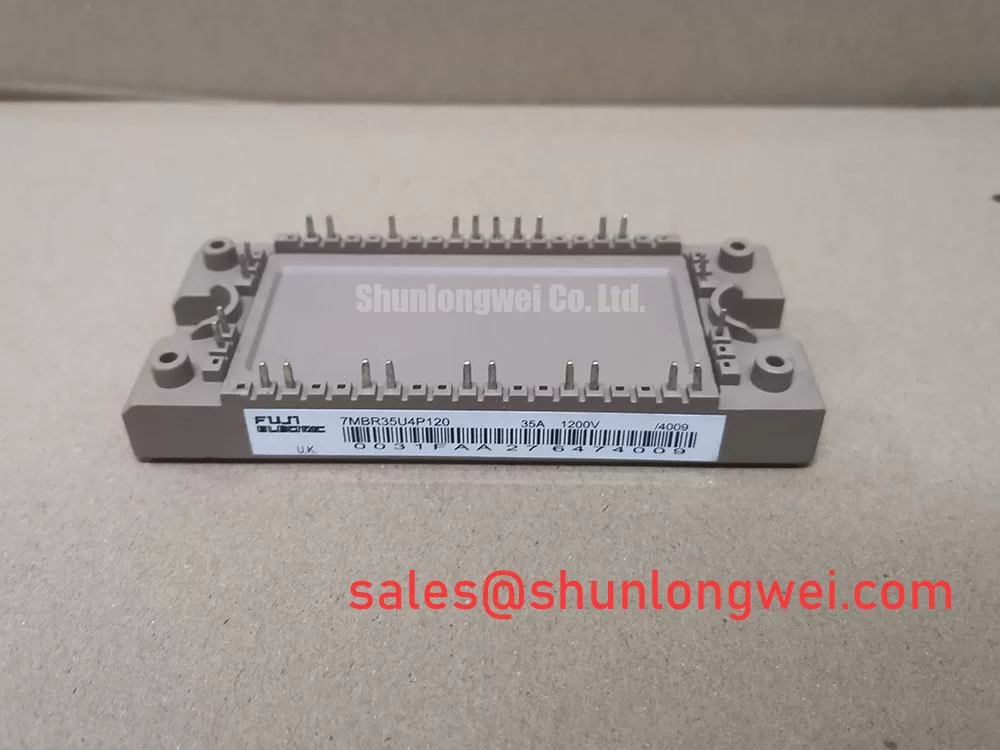
Engineering Recommendation: tune external gate resistance from measured switching waveforms rather than adopting a value from another drive. Gate driver source and sink capability, loop inductance, module temperature, and intended switching conditions influence ringing and switching loss. For cross model evaluation, 7MBR35UA120 is a related Fuji Electric module that should be compared against the original circuit schematic, terminal arrangement, protection method, and thermal interface before any service decision.
Preventing Spurious Faults: Transient Thermal Impedance Guidelines for 7MBR35SB120-01
The official inverter power dissipation is 240 W per device, yet safe pulsed operation depends on the time dependent thermal path from junction through the module base to the heat sink. Design Consideration: use the applicable manufacturer thermal impedance information and the actual pulse profile to assess transient junction temperature, rather than treating the continuous dissipation value as a pulsed overload allowance.
On a maintained drive, trend heat sink temperature and investigate changes after cleaning, fan replacement, cabinet sealing work, or a change in machine cycle time. Restricted airflow, uneven mounting pressure, aged interface material, or condensation can each alter thermal behavior without producing the same visible fault signature. Thermoelectric cooling concepts are discussed in this reference on the thermoelectric effect, but such cooling is a system design topic and is not an inherent feature of this module.
⚠️ Maintenance Note: Monitor contact temperature rise and confirm that the heat sink air path remains clear before returning a repaired drive to sustained production duty.
For broader reliability planning, the Power Electronics Masterclass outlines power semiconductor selection and system reliability considerations. It should complement, not replace, measured thermal verification on the actual actuator drive.
Benchtop Waveform Tuning: Mitigating Stress via DC Link Capacitance Bank Layout and Low ESR
During switching, peak device voltage rises above the DC link because stray inductance interacts with changing current. In engineering terms, the additional voltage is related to loop inductance multiplied by current change rate. Design Consideration: position the local DC link capacitor bank and power conductors to minimize the commutation loop area, then verify collector emitter overshoot with correctly referenced high voltage measurement equipment.
Bench testing should record DC link voltage, collector emitter waveform, gate emitter waveform, current, and fault behavior at representative operating conditions. Excessive ringing may indicate a layout issue, capacitor connection problem, gate damping mismatch, or measurement setup limitation. Avoid deciding from one waveform alone; compare the result with the known good signal path and the original drive’s switching conditions.
A larger module elsewhere in the power conversion chain, such as the 6MBI450U-120A-05, may serve a different rectifier or inverter duty and should not be treated as electrically interchangeable with the 7MBR35SB120-01. Confirm topology, control interface, protection coordination, thermal assembly, and the complete DC link arrangement before integration into a precision stepper or BLDC servo motion actuator.