Content last revised on September 10, 2026
Static Parameter Verification and Architecture of the 6MBI50U4A-120 Six-Pack Module
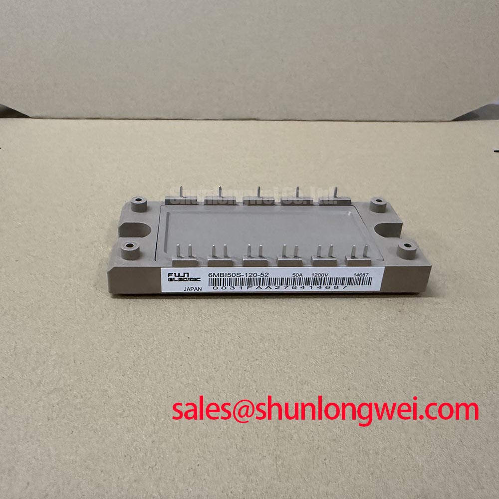
Incoming quality assurance for power conversion systems demands rigorous static parameter verification before any power stage assembly. The 6MBI50U4A-120, manufactured by Fuji Electric, is a 6-pack (three-phase inverter bridge) module integrating six IGBT cells and six fast-recovery antiparallel freewheeling diodes (FWDs) into a compact industrial package. Operating on high-stress industrial hardware such as medium-frequency induction heating supplies and multi-operator inverter welders requires technicians to verify terminal-to-terminal parameters right out of the anti-static packaging.
💡 Bench Tip: When checking unpowered modules on the test bench, always enforce electrostatic discharge (ESD) safeguards. Keep the gate and emitter pins shorted with conductive foam until gate threshold tests begin. Using a calibrated digital multimeter in diode-check mode, verify the cold-state forward voltage drop across each antiparallel diode (Emitter to Collector of each switch). A nominal reading of 0.35V to 0.48V at room temperature (25°C ambient) indicates intact internal bond wires and silicon junctions. Any open circuit reading (OL) or short circuit (under 0.05V) indicates junction degradation or catastrophic bonding lift-off.
| Parameter | Official Datasheet Specification | Engineering Significance |
|---|---|---|
| Collector-Emitter Voltage (VCES) | 1200V | Guarantees adequate breakdown headroom on rectified 380V to 480V three-phase AC industrial mains. |
| Continuous Collector Current (IC) | 50A (at TC = 80°C) | Defines steady-state thermal throughput capacity under typical industrial heatsink conditions. |
| Collector-Emitter Saturation Voltage (VCE(sat)) | 1.70V (typ. at Tj = 125°C, IC = 50A) | Minimizes conduction loss during heavy duty-cycle operations in welding and induction stages. |
| Topology / Configuration | Six-Pack (3-Phase Bridge) | Contains all three inverter half-bridges, eliminating external phase-to-phase link cabling. |
| Silicon Technology | 4th Gen. U4-Series Trench Gate | Refined carrier profile balances turn-off switching losses (Eoff) with lower EMI emissions. |
Compared to legacy planar modules like the 6MBI50J-120, the U4 trench architecture optimizes electron-hole plasma distribution near the emitter, yielding lower collector-emitter saturation voltage while maintaining a square Short-Circuit Safe Operating Area (SCSOA).
Mitigating Hard Switching Transients via Active Desaturation Soft Shutdown
In high-power industrial inverter welders, electrode short-to-workpiece events generate rapid, low-impedance fault currents. When an IGBT conducts into an uninhibited short circuit (Type I) or suffers a flashover across an inductive load during conduction (Type II), current escalates to five to eight times the continuous current rating within fractions of a microsecond. The 6MBI50U4A-120 is rated for a short-circuit withstand duration of tsc ≤ 10 µs under specified test conditions (VGE = 15V, VCC = 800V, Tj ≤ 125°C, Official Datasheet Specification).
Executing an abrupt gate discharge during this high-current fault condition induces extreme inductive voltage spikes. Because the stray inductance (Lσ) of the DC-link busbar reacts against the turn-off di/dt, terminating the gate voltage abruptly via standard low-impedance turn-off can generate transient voltages that easily exceed the 1200V VCES ceiling, puncturing the collector-emitter junction.
To safely isolate fault conditions, drive circuits must implement active two-stage desaturation detection and soft turn-off. A high-voltage blocking diode monitors the collector voltage when the gate is driven high. Once the blanking time (set typically between 1.5 µs and 3.0 µs to bypass the initial turn-on voltage tail) expires, if the collector voltage fails to collapse below the desaturation threshold (nominally set at 6.5V to 7.2V), the comparator trips the soft turn-off sequence. Instead of clamping the gate directly to -8V or 0V through the primary turn-off resistor, the driver switches in a soft-discharge resistor (typically RG,soft = 47 Ω to 100 Ω, Design Consideration) or drives a constant current sink of 50 mA to 100 mA. This controlled discharge gradually ramps down the channel current over a 2 µs to 4 µs window, attenuating the di/dt slope so that the resulting inductive spike stays safely within the 80% derating limit of VCES (≤ 960V).
⚠️ Field Alert: When retrofitting or replacing gate driver boards, never omit or reduce the desaturation sense diode's high-voltage isolation rating. The desat sense diode must withstand the full 1200V rail plus transient overshoots, with ultra-fast reverse recovery (trr < 75 ns) to prevent DC-link bus energy from back-feeding into the low-voltage logic core.
Multi-Module Parallel Current Sharing & Positive Tempco Dynamic Balancing
In medium-frequency induction heating units requiring output levels beyond the 50A rating of a single module, engineers frequently parallel multiple modules or parallel the internal legs. Balancing static and dynamic currents across silicon dies is critical to avoiding localized thermal runaway.
Static current sharing relies on the positive temperature coefficient of the saturation voltage. In the 6MBI50U4A-120, the U4 trench cell structure exhibits a slightly negative temperature coefficient at low collector currents (< 15A), which transitions into a strongly positive temperature coefficient above 20A. As junction temperature (Tj) rises from 25°C to 125°C under nominal load (IC = 50A), VCE(sat) increases from approximately 1.55V to 1.70V (Official Datasheet Specification). If one paralleled switch draws disproportionate current, its junction heats up, increasing its internal conduction resistance and naturally redirecting excess current into the cooler companion modules.
Dynamic current balancing during switching intervals requires strict symmetry in the physical gate drive and power loops. Differences of even 3 nH to 5 nH in loop inductance between paralleled gates can introduce switching time skews of 20 ns to 50 ns, causing the faster-turning-on module to shoulder the entire turn-on current spike. To maintain balance across all operating modes:
- Assign independent, dedicated series gate resistors (RG) to every individual gate terminal rather than driving multiple gates through a single shared resistor. Suggested starting value: RG = 15 Ω to 22 Ω (Typical Starting Point for bench tuning).
- Ensure Kelvin-emitter return paths for each gate loop trace directly back to their respective auxiliary emitter pins, preventing main emitter power currents from inducing common-source feedback voltages in the gate circuit.
- Coordinate circuit protection using ultra-fast semiconductor fuses. Fuse selection must ensure the clearing I2t of the fuse at line voltage remains strictly below the burst energy limits of the module housing to prevent catastrophic case rupture during continuous dead-short failures. Detailed failure mode evaluations and metallurgical inspections are documented in the Field Engineer’s Handbook.
Optocoupler vs Digital Coreless Transformer Isolation in High-Voltage Switching
High-voltage inverter topologies present severe common-mode noise hazards to control logic. In medium-frequency induction heating generators, switching edge speeds (dv/dt) frequently exceed 20 kV/µs to 40 kV/µs on the phase output nodes. This rapid potential shift injects displacement currents across the galvanic isolation barrier directly toward the secondary logic ground.
Standard optocouplers rely on light-emitting diodes and photodetectors separated by an insulating silicone or polyimide layer. While optocouplers offer reinforced isolation ratings (exceeding 3.75 kVRMS to 5.0 kVRMS), their common-mode transient immunity (CMTI) is fundamentally limited by parasitic barrier capacitance (Cio, often 0.5 pF to 1.2 pF). Under steep dv/dt conditions, displacement currents pass through this parasitic capacitance, causing signal jitter, false threshold transitions, or destructive latch-up in the primary-side microcontroller circuitry.
Modern industrial architectures increasingly utilize digital coreless transformer or capacitive galvanic isolation barriers. Coreless transformer isolators integrate differential receiver architectures with common-mode cancelation loops, achieving CMTI ratings exceeding 100 kV/µs to 150 kV/µs. Differential signal transmission rejects common-mode noise swings, keeping gate driver logic uncorrupted during aggressive hard-switching events. For discrete drive implementations and isolation circuit design notes, refer to the Fuji Electric High-Speed Discrete IGBTs overview.
Regardless of the chosen isolator technology, strict printed circuit board (PCB) creepage and clearance must be maintained beneath the isolation barrier. Maintain a minimum clearance distance of 8.0 mm and creepage across FR4 of at least 10.0 mm for Pollution Degree 2 environments operating up to 600V RMS working voltage, preventing track degradation caused by high-voltage surface stress.
Planar Symmetrical Busbar Geometry: Achieving Lσ < 20nH to Protect Silicon Junctions
Parasitic loop inductance within the DC-link path is a primary cause of overvoltage breakdown in 1200V IGBT applications. During turn-off, the rapid fall of collector current through the total parasitic loop inductance generates a severe overvoltage spike that superimposes onto the DC bus voltage. If the peak voltage exceeds the 1200V VCES absolute maximum rating, catastrophic avalanche breakdown occurs.
To constrain this transient within safe operating boundaries, designers must limit parasitic inductance through optimized planar symmetrical busbars. The DC bus routing must utilize wide, thin copper plates separated by thin layers of high-dielectric insulation (such as 0.25 mm to 0.5 mm Mylar or Nomex sheet). Arranging the positive (DC+) and negative (DC-) laminated bus conductors in close physical proximity maximizes magnetic flux cancellation, cutting total busbar inductance down below 20 nH.
A high-frequency polypropylene film snubber capacitor (typically 0.47 µF to 1.0 µF / 1200V DC) should be mounted directly across the DC+ and DC- terminals of the module, utilizing low-inductance terminals. For additional structural recommendations and layout examples, consult the Fuji Electric V-Series IGBT Application Manual.
Thermal mounting is equally crucial to maintaining reliability under cyclic industrial loads. Apply a uniform, screen-printed layer of thermal interface material (TIM) with a target thickness of 50 µm to 100 µm across the module's copper baseplate. Excessive grease thickness increases junction-to-case thermal resistance (Rth(j-c)), while insufficient grease creates air voids that impede heat extraction.
Tighten the M5 heatsink mounting screws progressively in a crosswise pattern. Apply an initial torque of 1.0 N·m across all mounting points, followed by a final tightening torque of 2.5 N·m to 3.5 N·m (General Industry Design Consideration for M5 module mounting screws). This controlled compression flattens the module baseplate evenly against the heatsink surface, ensuring minimal thermal contact resistance and preventing mechanical warping of internal ceramic substrates under high thermal cycling.