

Content last revised on November 4, 2026
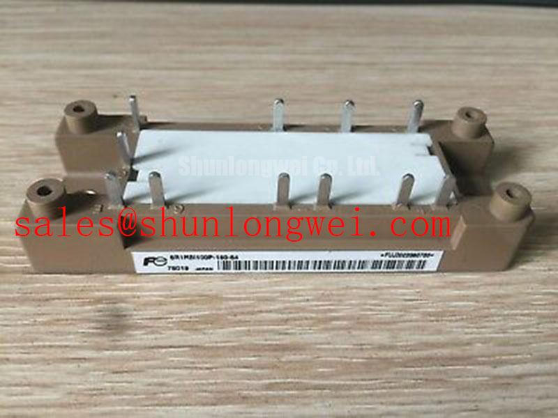
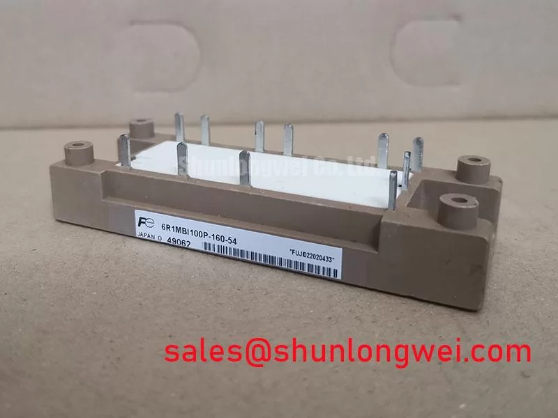
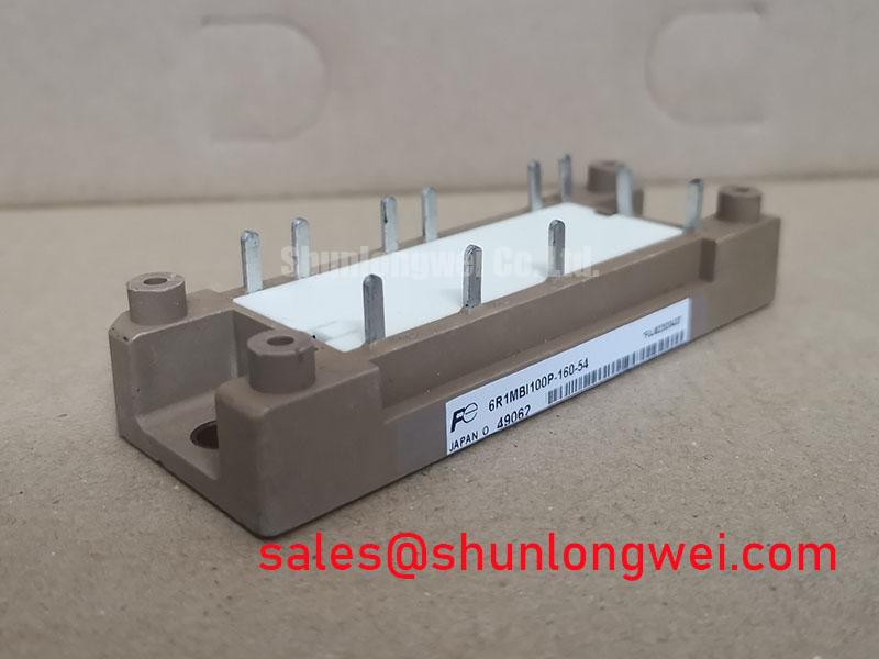
6R1MBI100P-160-54 Thermal-Electrical Optimization: Diagnosing Latent Gate-Emitter Dielectric Practical Tuning
Cold unpowered screening should start with terminal identification rather than a powered functional test. Confirm the collector, emitter, and gate connections from the equipment documentation, then use the diode-check function to examine the main semiconductor paths in both polarities. The antiparallel diode should be assessed as a junction path with a directional response, while the IGBT path should not be interpreted from one isolated meter reading. Different meters apply different test currents, so the useful comparison is repeatability against a reference device and consistency across the complete terminal set.
Gate leakage screening requires a controlled instrument setup. Discharge the module, remove the gate-drive connector, and prevent the meter from injecting an unintended charge into the gate. Measure gate-to-emitter and gate-to-collector behavior with the power terminals isolated. A changing indication can result from stored charge, test-lead capacitance, contamination, or a damaged dielectric path. Let the reading settle, repeat with reversed lead placement where appropriate, and document the result instead of assigning a failure mode from a single display value.
The thermal and electrical relationship becomes important once the module is returned to a converter. Excess junction temperature changes switching behavior and can increase stress on the gate-drive loop, while a poor gate reference can create apparent thermal symptoms through incomplete or delayed switching. Designers should verify the actual gate waveform at the module terminals, including turn-on, turn-off, Miller-region behavior, and the relationship between the gate-emitter reference and the power emitter. The gate-drive return path should be kept separate from high-current commutation paths until the intended connection point.
For a commercial string inverter or micro-grid energy-storage converter, the system integrator should review the boost stage, inverter bridge, and DC-link charging sequence together. A bootstrap or auxiliary gate supply needs sufficient charge recovery during the available switching interval, and its diode reverse-recovery behavior should be assessed against the driver frequency and load current. The correct supply voltage must be taken from the original gate-driver documentation rather than inferred from the IGBT module rating. Dead-time settings should be validated with current and voltage probes so that cross-conduction protection does not create excessive diode conduction or abnormal switching loss.
When a replacement is being evaluated, compare electrical topology, gate-drive reference, diode direction, terminal spacing, cooling interface, and protection coordination as a complete set. The 2MBI200S-120 may be reviewed as a separate Fuji module option where the system topology and verified ratings are compatible, but its suitability must be established from the equipment documentation and the relevant component data.
Assembly Integrity & Layout Architecture: Optimizing Heatsink Contact Pressure and Spacing for 6R1MBI100P-160-54
Thermal interface preparation determines how effectively heat leaves the module baseplate. Clean both mating surfaces, inspect the heatsink for local distortion, and apply the selected thermal interface material as a continuous, controlled layer. A common design consideration is to control the interface thickness within the material supplier’s stated application window; the supplied engineering outline identifies 50 to 100 micrometres as a possible working range, but this is not a Fuji Electric factory specification for the module. Voids, foreign particles, and uneven spreading can create local thermal resistance that will not be visible from an electrical bench test.
Baseplate curvature should be checked before final tightening. A straightedge, surface plate, or the equipment manufacturer’s approved inspection method can reveal a contact pattern that is concentrated near one edge. Correct the mechanical condition before installing the module. Do not use screw force to compensate for a severely distorted heatsink, because excessive local pressure can transfer stress into the package and produce uneven thermal contact.
Use a crosswise, sequential tightening pattern and the original mechanical documentation for the permitted fastening torque. The supplied 2.5 to 3.5 N·m range may be treated only as a general M5 mounting design consideration where applicable, not as an official rating for this specific Fuji module. Thread condition, washer arrangement, heatsink material, screw grade, and the module’s mounting instructions all affect the final assembly method. Recheck the interface after the initial thermal cycle if the equipment procedure calls for it.
Electrical layout should keep the high-current commutation loop compact and physically separated from sensitive gate-drive traces. The engineering target of 25 nH or less for a busbar loop is a system design consideration supplied for this application brief, not a published module specification. The correct objective is to minimize parasitic inductance and verify the resulting turn-off overshoot during switching tests. A film snubber should be placed close to the commutation path it is intended to control, with short, wide connections and a return path that does not add a separate high-inductance loop.
Long motor cables, transformer leakage, and filter components can produce reflected or resonant voltage behavior in an inverter installation. The layout review should therefore include the complete path from the DC link through the module, output filter, cable, and motor or storage interface. Any filter or damping network must be selected from measured ringing, switching frequency, insulation coordination, and thermal loss. The module’s 1600 V rating should not be treated as permission to ignore transient measurement at the actual terminals.
The front-end rectifier also affects the stress seen by the inverter bridge. Phase-controlled rectification, DC-link charging, and grid impedance can shape current distortion and capacitor ripple. A compatible system may evaluate a separate rectifier-stage component such as 1MBI400L-120, but that device is a neutral reference for topology discussion, not an automatic companion or prescribed replacement for the 6R1MBI100P-160-54.
Benchtop Waveform Tuning: Mitigating Stress via Type-2 Coordination and Protecting the IGBT Module on 6R1MBI100P-160-54
Protection coordination should be tested as a timed event involving the semiconductor, the fuse, the DC-link capacitor, and the gate driver. A high-speed semiconductor fuse must interrupt the available fault energy before the module experiences destructive electrical or mechanical stress. Compare the fuse total-clearing I2t with the module manufacturer’s permitted short-circuit and overload conditions, using the actual prospective fault current and DC-link arrangement rather than a nominal fuse label.
During a controlled test, capture gate voltage, collector-emitter voltage, phase current, and the protection command on a common time base. The useful question is whether the gate is driven to the intended off state quickly enough while the fuse and contactor sequence prevent continued energy delivery. Probe placement matters: long ground leads can create an apparent overshoot that is not present at the module terminals, while an incorrectly referenced gate probe can hide a real transient.
Type-2 coordination requires attention to the boundary between a cleared fault and a damaged but still conductive module. Check whether the gate driver detects desaturation, overcurrent, or supply abnormality before the fuse reaches its clearing interval. The system designer should confirm that the protection chain does not depend on a controller restart after the semiconductor has already entered an uncontrolled state. Any reset sequence should require the DC link to be discharged and the fault cause assessed before re-energization.
Gate-loop inductance, driver output impedance, and negative off-bias behavior can influence turn-off speed and voltage overshoot. The technical guide Evolution of Negative Off-Bias Gate Drive Circuits provides relevant background for evaluating negative off-bias arrangements. It should be used alongside the original driver and module documentation because the correct gate-voltage limits, isolation method, and protection timing belong to the complete gate-drive design.
The Fuji Electric reference material for Power Semiconductor and IPM Modules and the Fuji Electric PIM Power Integrated Module family can help place the module within the manufacturer’s broader power-semiconductor portfolio. These references do not replace the exact data for this part or establish a system-level protection guarantee.
Benchtop Waveform Tuning: Preventing Terminal Overheating During Operation on 6R1MBI100P-160-54
Terminal heating should be investigated at the bolted joint, the conductor interface, and the module terminal itself. Use a calibrated micro-ohmmeter with a four-wire connection to measure the assembled joint after power isolation and discharge. The supplied 10 micro-ohm value is a general engineering screening target for a bolted high-current connection, not an official Fuji Electric terminal specification for this model. The measurement should be repeated after mechanical inspection because probe placement, surface condition, and parallel current paths can materially change the result.
Inspect the contact surfaces for contamination, oxidation, burrs, damaged plating, or uneven washer pressure. Confirm that the cable lug sits flat and that the conductor is not exerting side load on the terminal. A joint can show an acceptable cold resistance while developing an abnormal temperature rise under load if the current distribution is uneven or the mechanical pressure relaxes during operation.
Thermographic testing should be performed after the converter reaches a representative continuous-load condition. Compare the module terminals, busbar transitions, fuse connections, and neighboring phase conductors under the same load and airflow. A localized temperature difference is a prompt for further electrical and mechanical inspection, not proof of one specific failure mechanism. Correlate the thermal image with current measurement and voltage drop across the joint.
For a commercial string inverter or micro-grid storage system, review terminal heating during startup, steady-state power transfer, regenerative operation, and grid-support transitions. The current waveform may change substantially when the converter shifts between charging and discharging, and the hottest connection may not be the one nearest the module. Check the DC-link ripple, switching balance, cooling airflow, and enclosure temperature as part of the same test record.
Before returning the assembly to service, verify that the gate connector is fully seated, the power terminals are tightened according to the approved mechanical procedure, and all protective covers preserve the required electrical clearance. Field Alert: Never connect or remove the gate-drive cable while the DC link or auxiliary gate supply remains energized.