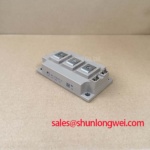
Content last revised on August 29, 2026
Junction-to-Case Thermal Network Simulation under High-Pulsed Overloads
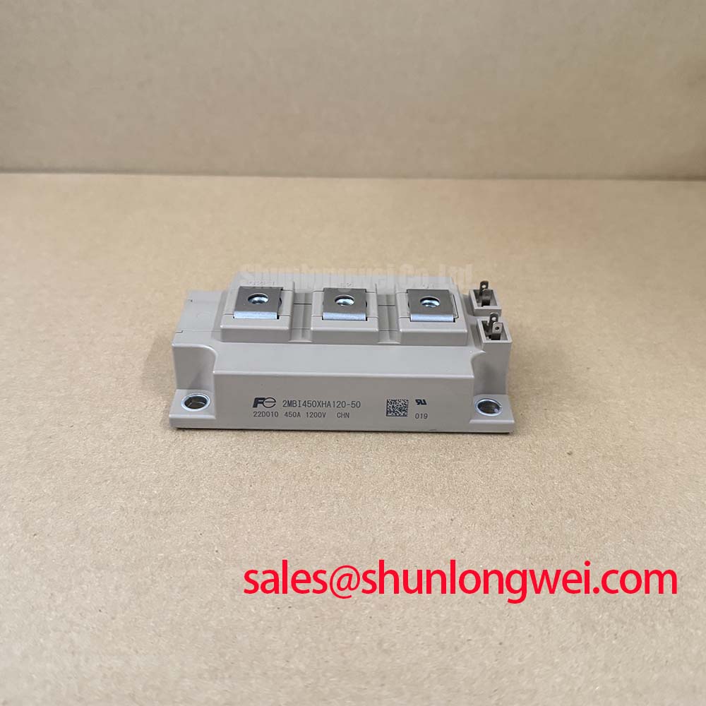
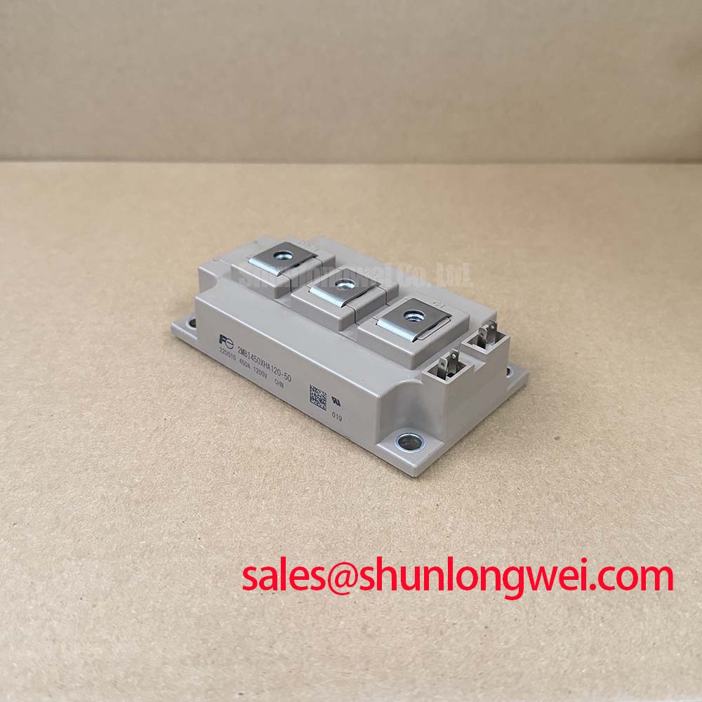
Evaluating high-power dual IGBT modules on the incoming inspection bench requires careful verification of both electrical tolerances and physical thermal boundaries. The Fuji Electric 2MBI450XHA120-50 is rated for a collector-emitter voltage VCES = 1200V and a continuous collector current IC = 450A at a case temperature of TC = 85°C (Official Datasheet Specification). In demanding multi-axis CNC milling centers and robotic articulated arms, drives do not operate under constant steady-state conditions. Instead, they face severe transient acceleration surges where collector peak currents reach repetitive spikes up to ICRM = 900A for 1 ms durations (Official Datasheet Specification).
When simulating and testing transient thermal impedance, incoming QA engineers must analyze how short-duration pulsed power relates to the module total power dissipation rating of Ptot = 1850W per single device (Official Datasheet Specification). Under high-torque dynamic axis reversal, the instantaneous thermal energy generated in the sub-micron silicon channels transfers through the direct copper bonded (DCB) ceramic substrate to the copper baseplate. To evaluate transient temperature rises without exceeding the maximum operating virtual junction temperature rating of Tvjop = -40°C to +175°C (Official Datasheet Specification), technicians utilize multi-element Foster and Cauer RC network models. These models map the individual time constants of the silicon die, solder layer, ceramic isolation, and baseplate structure.
When benchmarking new assemblies or evaluating replacements against previous-generation platforms such as the 2MBI450U4N120-50, thermal interface material (TIM) application plays a decisive role. The published thermal resistance case-to-sink is Rth(c-s)} = 0.121 K/W when using standard thermal grease (Official Datasheet Specification). On the bench, verifying baseplate flatness and applying a uniform 100 µm screen-printed grease layer prevents localized hot spots that induce cyclic solder fatigue across high-dynamic duty cycles.
💡 Bench Tip: Before placing high-power modules into automated test fixtures, always perform a preliminary cold-state multimeter diode-drop check across the terminals. With gate and emitter terminals shorted to avoid ESD floating bias, measure the anti-parallel free-wheeling diode forward on-voltage drop. At 25°C room ambient, a healthy unit presents an initial cold forward drop close to the rated nominal forward voltage VF = 1.70V (typical, terminal) (Official Datasheet Specification). Significant deviation from terminal specifications indicates structural degradation or internal bond-wire imbalance.
High dv/dt Cross-Conduction Shoot-Through Mitigation via Dedicated Miller Clamps
Modern fast-switching industrial drive designs minimize switching losses by operating at aggressive slew rates. However, in half-bridge configurations driving servo motors, rapid collector-emitter voltage transients (high dv/dt) on the switching IGBT induce capacitive displacement currents through the internal parasitic Miller capacitance (Cres / Cgc) of the complementary inactive switch. The 2MBI450XHA120-50 exhibits an input capacitance of Cies = 46nF (typical) (Official Datasheet Specification), which must be actively managed to prevent parasitic turn-on and catastrophic DC-bus shoot-through.
To safely suppress induced voltage spikes at the gate terminal during high-speed switching, gate driver boards require two complementary protection layers: stable negative turn-off bias and low-impedance active Miller clamping circuits. Operating the gate driver with an off-state negative bias between -5V and -15V (with -8V to -10V serving as a Typical Starting Point for bench tuning) expands the threshold margin well above the internal gate-emitter threshold voltage. Furthermore, when the collector-emitter voltage rises abruptly across the low-side switch, the active Miller clamp circuit detects the falling gate edge and engages an auxiliary low-impedance MOSFET to shunt displacement current directly to the negative rail, bypassing the primary turn-off gate resistor.
In addition to active clamping, layout parasitic mitigation remains critical. Engineers should refer to industry-standard topologies documented across the Fuji Electric Power Semiconductors Portal to implement dedicated Kelvin emitter connections. Isolating the high-current power return loop from the low-power gate drive reference prevents ground-bounce transients from degrading driver signal integrity during multi-axis servo accelerations. For comprehensive bench validation procedures and gate-oxide degradation analysis, refer to our compiled Field Engineer’s Handbook.
Regenerative DC-Bus Voltage Surge Dissipation during Rapid Machine Deceleration
In CNC spindle braking and robotic axis deceleration, kinetic energy stored in the mechanical load is converted back into electrical energy by the permanent magnet synchronous motor (PMSM). This regenerated energy flows through the module's anti-parallel free-wheeling diodes and charges the primary DC-link capacitor bank, causing a steep rise in DC-bus voltage. Because the absolute maximum rating for collector-emitter voltage is VCES = 1200V (Official Datasheet Specification), unmanaged bus surges can easily exceed the avalanche breakdown limits of the silicon die.
Under nominal 400V/480V AC utility feeds, the rectified steady-state DC bus operates between 560V and 680V. During aggressive braking cycles, a dynamic braking chopper circuit must engage when the bus reaches approximately 750V to 780V, directing surge energy into heavy-duty ballast resistors. While the main inverter stages employ heavy modules like the 2MBI450XHA120-50, auxiliary braking choppers or lower-voltage auxiliary rails often coordinate alongside complementary power topologies such as the 2MBI400VB-060-50.
⚠️ Field Alert: When mounting power modules to liquid-cooled or forced-air heatsinks, follow strict torque sequences. An M5 mounting bolt requires a tightening torque of 2.5 to 3.5 N·m (General Industry Design Consideration for M5 hardware). Uneven torque application warps the internal ceramic substrate, introducing mechanical stress cracks that degrade galvanic isolation and cause localized thermal runaway during full-load regenerative cycles.
The table below summarizes the key baseline electrical and thermal parameters verified during incoming component qualification for the 2MBI450XHA120-50 module:
| Parameter | Symbol | Datasheet Value | Condition / Note |
|---|---|---|---|
| Collector-Emitter Voltage | VCES | 1200 V | Official Datasheet Specification |
| Continuous Collector Current | IC | 450 A | TC = 85°C (Official Specification) |
| Repetitive Peak Current | ICRM | 900 A | tp = 1 ms (Official Specification) |
| Saturation Voltage (Terminal) | VCE(sat) | 1.65 V (typ) | IC = 450A, VGE = 15V (Official Specification) |
| FWD Forward Voltage Drop | VF | 1.70 V (typ) | IF = 450A, Terminal (Official Specification) |
| Input Capacitance | Cies | 46 nF (typ) | VCE = 10V, VGE = 0V, f = 1MHz |
| Max Power Dissipation | Ptot | 1850 W | 1 device (Official Specification) |
| Operating Junction Temp | Tvjop | -40 to +175 °C | Official Datasheet Specification |
| Isolation Voltage | Visol | 4000 V AC | 1 min, 50/60 Hz (Official Specification) |
Long Motor Lead Reflected Wave Voltage & Motor Terminal Insulation Protection
Industrial automation installations frequently position the variable frequency drive cabinet tens of meters away from the servo motors situated on robotic gantries. This transmission line setup creates an impedance mismatch between the shielded motor cable and the high-impedance motor stator windings. When the steep switching edges of the 2MBI450XHA120-50 propagate down long cables, voltage reflections can double the peak amplitude at the motor terminals, creating spikes approaching twice the DC-link voltage.
To preserve both the motor winding insulation and the power module output stage, system designers incorporate output dv/dt filters, ferrite common-mode chokes, or sinusoidal output filters. Sizing these filters limits output voltage rise times to below 500 V/µs (General Industry Design Consideration for standard AC industrial motors), eliminating localized inter-turn dielectric breakdown. On the power module side, the unit's galvanic isolation capability is confirmed by an official factory test rating of Visol = 4000V AC for 1 minute between the baseplate and electrical terminals (Official Datasheet Specification).
Incoming quality control protocols require routine verification of terminal-to-baseplate isolation resistance using high-voltage insulation testers (typically applied at 2.5kV DC for 60 seconds) to ensure the internal DCB ceramic barrier has not suffered micro-fracturing during freight handling. Maintaining clear electrical clearance paths and creepage distances around power busbars prevents tracking discharge across high-voltage industrial enclosures exposed to conductive dust and atmospheric humidity.