Content last revised on September 10, 2026
Product Overview: 6MBI450V-170 6-Pack Power Module
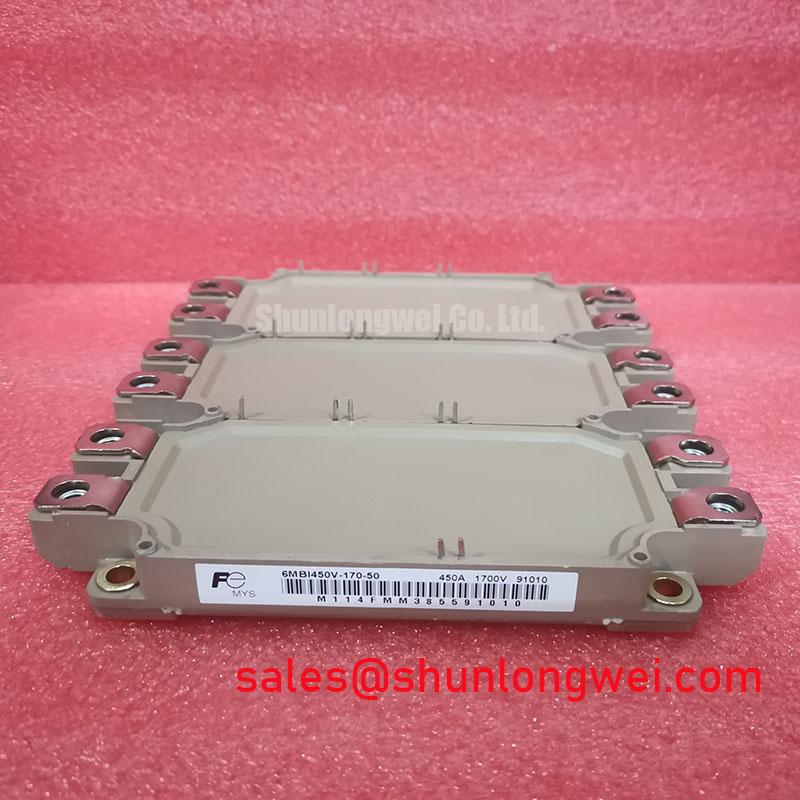
The 6MBI450V-170 is a high-power six-pack (three-phase bridge) IGBT module developed by Fuji Electric, designed for high-reliability conversion topologies such as Commercial & Industrial (C&I) Battery Energy Storage Power Conversion Systems (PCS) and medium-voltage industrial drives. Integrating six insulated gate bipolar transistors and fast-recovery freewheeling diodes (FWD) into a single mechanical housing, the 6MBI450V-170 optimizes thermal distribution and mechanical footprint across three-phase power stages.
| Parameter | Specification Value | Engineering Significance |
|---|---|---|
| Collector-Emitter Voltage (VCES) | 1700V | Provides high voltage breakdown margins for 690V AC line systems and 1000V–1100V DC-link buses. |
| Continuous Collector Current (IC) | 450A (at TC = 80°C) | Handles nominal continuous current demands in multi-hundred kilowatt PCS inverter bridges. |
| Repetitive Peak Collector Current (ICRM) | 900A | Absorbs short-duration fault surges, grid-tie reactive transients, and sub-cycle overload pulses. |
| Maximum Junction Temperature (Tj(max)) | 175°C | Extends thermal headroom during peak charge/discharge duty cycles, improving cycling reliability. |
| Circuit Topology | 6-Pack (Three-Phase Bridge) | Minimizes inter-switch busbar routing, reducing overall assembly parasitics and mechanical complexity. |
Fault-Clearing Dynamics: Type-I/II Desaturation Detection and Inductive Clamping
In bidirectional battery storage PCS applications, line-to-line faults or internal bridge short circuits present severe current transients that test the Short-Circuit Safe Operating Area (SCSOA). The 6MBI450V-170 provides a guaranteed short-circuit withstand capability (typically within tsc ≤ 10 µs under specified test conditions). Fault profiles are categorized into Type-I (turn-on into an existing dead short) and Type-II (short-circuit occurring while the device is in the fully conducting state).
Under a Type-II fault, the collector-emitter voltage rises abruptly from its nominal saturation level VCE(sat) toward the DC-bus voltage VDC while conducting maximum fault current. The gate-drive subsystem must execute desaturation detection (DESAT) via a high-voltage blocking diode. As specified in the Fuji Electric V-Series IGBT Application Manual, hard gate turn-off during peak desaturation currents risks catastrophic overvoltage breakdown due to rapid di/dt across the stray parasitic loop inductance Lsigma:
Vpeak = VDC + Lsigma · (di/dt)
To keep Vpeak below the 1700V VCES threshold, gate drivers must implement active two-stage soft turn-off (2STO) or intermediate gate voltage clamping. By ramping the gate down slowly, di/dt is constrained, preventing excessive voltage spikes before inductive energy dissipates safely.
DC-Bus Operating Voltage Headroom Derating for Single Event Burnout (SEB) Immunity
Utility and commercial battery installations located at high altitudes (>2000 m) face increased cosmic ray exposure. High-energy atmospheric neutrons colliding with the silicon lattice can trigger localized avalanche breakdown, leading to Single Event Burnout (SEB) without prior thermal warning. The Failure in Time (FIT) rate for cosmic-ray-induced SEB depends exponentially on the applied electric field across the drift region.
For systems operating on a 900V to 1100V nominal DC-bus, a 1200V-rated power switch offers limited headroom against transient overvoltages and neutron-induced SEB. Utilizing the 6MBI450V-170 with its 1700V rating allows system architects to maintain DC-link utilization below 65% of rated VCES. This derating margin suppresses the terrestrial neutron FIT rate to single-digit values per megawatt-hour of operation. For systems requiring lower DC-bus limits where 1200V silicon is structurally sufficient, the related 2MBI450XHA120-50 provides dual-pack 1200V / 450A capability within an alternate packaging format.
Evaluating Thermal Capacitance vs Heat Sink Time Constant under Surge Bursts
Grid-support functions such as synthetic inertia and primary frequency regulation subject PCS inverters to high-current pulse bursts (e.g., 200% nominal load for 500 ms to 2 s). During these short intervals, the external liquid cold plate or forced-air heatsink cannot immediately respond due to its large thermal time constant (tausink in the range of tens of seconds).
The transient junction temperature Tj is governed by the multi-RC thermal impedance network (Foster or Cauer representation) defined by the junction-to-case thermal resistance Rth(j-c) and internal thermal capacitance Cth:
Tj(peak) = TC + Ploss(surge) · Zth(j-c)(t)
Because the 6MBI450V-170 provides an extended maximum junction temperature of 175°C, it delivers a broader delta-Tj margin during high-energy burst cycling. Evaluating these localized thermal cycles is critical to preventing bond-wire shear and solder fatigue, as detailed in comprehensive reliability protocols found in the Field Engineer’s Handbook.
PCB Symmetry Considerations for Dual IGBT Half-Bridge Switching Paths
Integrating a complete 6-pack inverter stage in one housing demands strict symmetry in gate-drive printed circuit board (PCB) layouts. Parasitic inductances in the power terminals and gate loops can lead to current imbalances, parasitic oscillations, and elevated dynamic switching losses (Eon, Eoff).
- Kelvin Emitter Separation: Auxiliary emitter connections must remain completely isolated from high-current power return paths to eliminate mutual inductive feedback: Vge(eff) = Vgate - LE · (di/dt).
- Gate Loop Parasitic Reduction: Minimizing the physical loop area between the gate trace and auxiliary emitter return limits stray inductance, preventing high dv/dt induced spurious turn-on via the Miller capacitance Cres.
- Balanced Gate Charge Delivery: Matching gate path impedance across all six positions ensures uniform total gate charge (Qg) transfer, suppressing phase-to-phase switching skew during PWM transitions.