Content last revised on September 10, 2026
Common-Mode Transient Immunity (CMTI > 100kV/us) in Harsh Industrial Environments
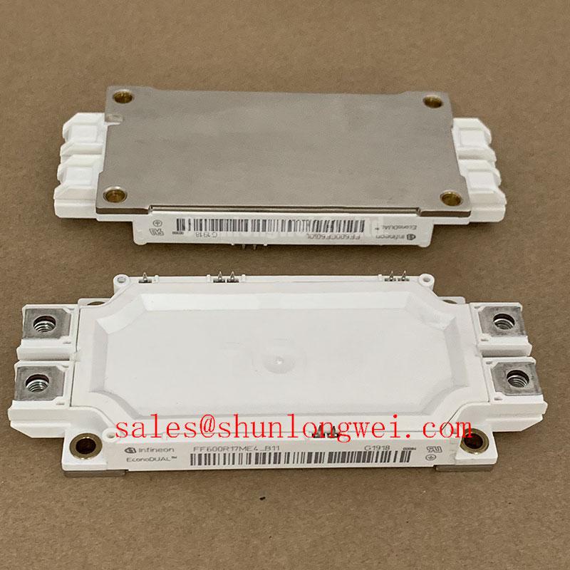
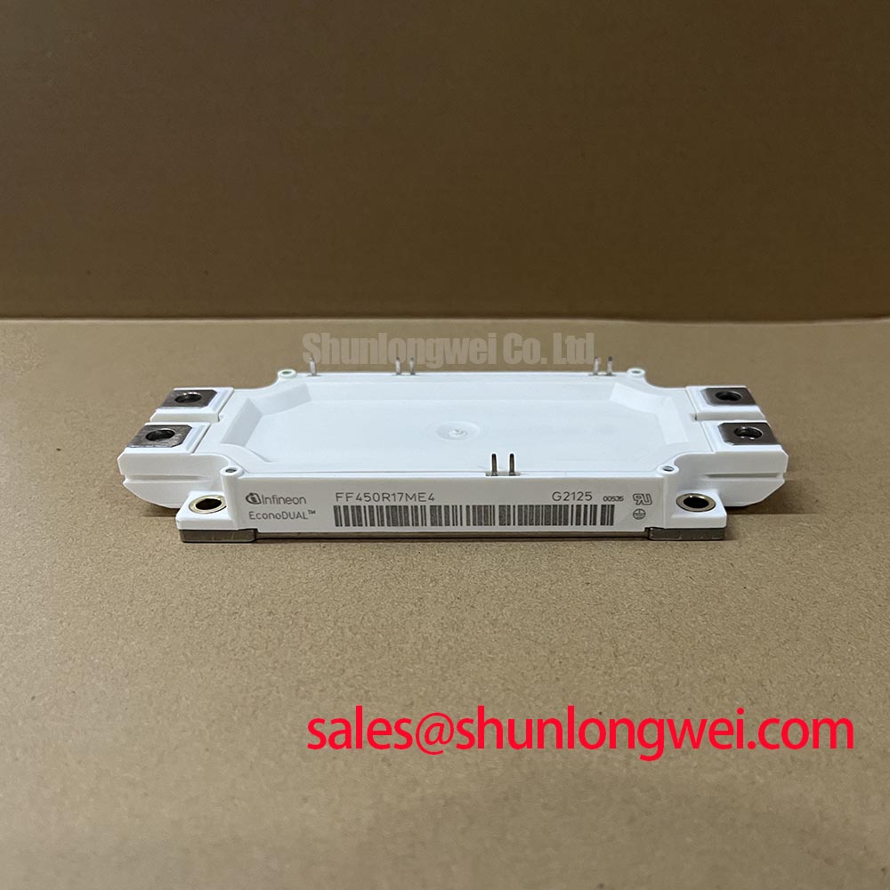
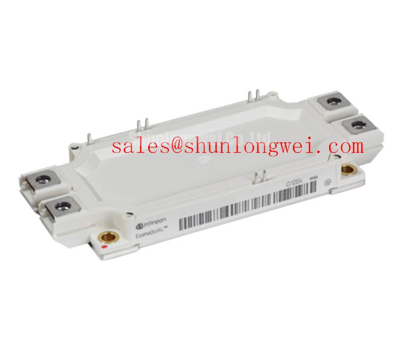
When responding to an unexpected fault trip on a utility-scale battery energy storage system (BESS) power conversion system (PCS), field technicians frequently encounter phantom desaturation alarms or erratic gate driver behavior. In high-power centralized PCS architectures operating across a 1500V DC link, fast-switching transitions generate common-mode voltage steps across the galvanic isolation barrier. The FF450R17ME3 is an industry-standard dual IGBT module rated at 1700V collector-emitter breakdown voltage and 450A continuous collector current (Official Datasheet Specification). Operating this silicon in high-capacity bidirectional inverters requires gate driver isolation stages capable of withstanding severe common-mode slew rates without corrupting control logic.
High-voltage utility conversions produce steep switching edges where transient rates often exceed 10kV/µs under heavy load commutations. When displacement currents cross the internal isolation barrier capacitance of the driver board, they induce common-mode transient noise that can falsify secondary-side logic signals. To maintain reliable operation, gate drive circuitry paired with the FF450R17ME3 must utilize reinforced galvanic isolation barriers exceeding 5kV isolation test voltage with a common-mode transient immunity (CMTI) threshold rating of at least 100kV/µs. Field remediation of nuisance driver faults begins with verifying the physical layout clearances: keep primary and secondary ground planes strictly separated with a minimum creepage and clearance distance of 12mm across the isolation boundary.
On-site diagnostics of suspected gate noise require high-bandwidth differential probes to measure the gate-to-emitter terminal pins directly at the module auxiliary contacts. If high-frequency ringing exceeding 2.5V peak is observed during turn-off transitions, check the common-mode choke implementation on the isolated DC-DC driver power rails. Suppressing transient ground displacement currents prevents false logic state transitions, protecting the inverter bridge from cross-conduction events during rapid power-flow reversals between grid charge and discharge cycles.
Multi-Module Parallel Current Sharing & Positive Tempco Dynamic Balancing
Centralized utility BESS inverters regularly parallel multiple half-bridge modules per phase leg to scale megawatt output. In these systems, ensuring balanced current distribution across all parallel semiconductor channels under static and dynamic conditions is vital to avoid localized thermal runaway. The FF450R17ME3 utilizes an advanced trench-field-stop IGBT chip design that exhibits a distinct positive temperature coefficient (positive Tempco) for on-state saturation voltage VCE(sat) above its rated nominal current. At an operating junction temperature of 125°C, the on-state voltage drop increases predictably with current (Official Datasheet Specification: typical VCE(sat) is approximately 2.0V at 450A), naturally driving current away from hotter dice and forcing static thermal equilibrium across paralleled modules.
While static current sharing is self-stabilizing due to silicon physics, dynamic current sharing during turn-on and turn-off transients depends entirely on hardware symmetry. Mismatched gate trace lengths, uneven busbar geometry, or unequal parasitic stray loop inductances will cause one module to switch faster than its parallel twin, subjecting the faster module to destructive turn-off energy concentrations. When replacing failed units during an emergency field rebuild, ensure that all paralleled modules share identical gate resistor values (Suggested initial gate damping: 3.3 Ω to 5.1 Ω as a Typical Starting Point for bench tuning) and that driver signal harnesses match in physical length within a tolerance of ±5mm.
| Key Parameter | Datasheet Value (Official Specification) | Field Verification Condition |
|---|---|---|
| Collector-Emitter Voltage (VCES) | 1700 V | Tvj = 25°C, Gate-Emitter Shorted |
| Continuous DC Collector Current (IC) | 450 A | TC = 80°C, Continuous Operation |
| Collector-Emitter Saturation Voltage (VCE(sat)) | 2.00 V (typ.) | IC = 450 A, VGE = 15V, Tvj = 125°C |
| Gate Charge (QG) | 4.4 µC (typ.) | VGE = -15V to +15V |
For systems experiencing regular thermal over-stress or requiring higher power headroom during inverter repowering, engineers can evaluate the structurally compatible FF650R17IE4DP_B2, which offers an upgraded 650A current handling capacity in a matching format. Desaturation (VCE(sat)) short-circuit detection networks must be calibrated to blank initial turn-on spikes for 2.5µs to 3.0µs before asserting fault conditions. In the event of a severe low-impedance DC short, the driver must execute a two-stage soft turn-off (2SSTO) within 3µs to softly reduce collector current, dampening the terminal overvoltage spike caused by busbar stray inductance Lσ.
Active Miller Clamp Implementation & Parasitic Capacitive Turn-On Prevention
In high-voltage half-bridge switching cells, rapid displacement current flows through the internal Miller capacitance (reverse transfer capacitance Cres) during complementary device switching. When the upper switch turns on with an aggressive collector-emitter voltage rise rate (dv/dt), the lower switch experiences high-frequency displacement current injected directly into its gate node. If the gate impedance is not low enough, this current charges the gate-emitter capacitance above the gate threshold voltage VGE(th) (Official Datasheet Specification: 5.2V to 6.4V), triggering instantaneous shoot-through and catastrophic cross-conduction failure.
To eliminate parasitic turn-on risks without sacrificing switching efficiency through oversized turn-off gate resistors, an Active Miller Clamp circuit is necessary. The active clamp dynamically bypasses the turn-off resistor by activating an ultra-low-impedance internal transistor once the gate voltage falls below approximately 2.0V relative to the negative rail. Furthermore, establishing a robust negative gate bias of -8V to -15V ensures sufficient noise margin below the gate threshold during all high-dv/dt commutation windows.
⚠️ Field Alert: When seating the module on the liquid cold plate during inverter overhauls, strictly adhere to thermal interface compound guidelines. Apply a uniform, screen-printed thermal paste thickness between 50µm and 80µm. Uneven grease application leads to air voids, increasing junction-to-case transient thermal impedance Zth(j-c) and causing localized die hotspots. Fasten the M5 mounting bolts using an initial cross-pattern pre-torque of 2.0 N·m, followed by a final calibrated torque of 3.0 N·m to 5.0 N·m (General Industry Design Consideration for M5 module mounting) to prevent substrate cracking.
Complementary free-wheeling diodes must exhibit an optimized reverse recovery softness factor S (the ratio of recovery decay time tb to peak current rise time ta) to prevent steep current snaps that radiate broadband electromagnetic interference (EMI). The integrated emitter-controlled diode inside the FF450R17ME3 provides soft recovery dynamics, mitigating excessive voltage overshoots across the laminated DC busbar under heavy full-load reverse power cycling.
DC-Bus Operating Voltage Headroom Derating for Single Event Burnout (SEB) Immunity
Centralized utility-scale energy storage plants are frequently installed in high-altitude desert and mountainous regions exceeding 2000 meters above sea level. At elevated altitudes, terrestrial cosmic ray neutron flux increases significantly, escalating the statistical risk of Single Event Burnout (SEB) inside high-power silicon dies. High-energy atmospheric neutrons colliding with the high-field depletion region of an off-state IGBT can trigger localized avalanche multiplication, leading to sudden, unrecoverable breakdown below the maximum rated VCES limits.
Field failure analysis protocols outlined in the Field Engineer’s Handbook highlight that cosmic-ray-induced Failure In Time (FIT) rates scale exponentially with applied DC-link voltage. While the FF450R17ME3 is rated for a peak breakdown of 1700V, industrial PCS designs maintain a continuous operational DC-bus voltage headroom derated to between 900V and 1100V (Design Consideration for high-reliability altitude deployment). Operating within this window ensures that neutron-induced FIT rates remain negligible over multi-decade system lifespans while providing sufficient voltage margin for transient inductive spikes generated during grid-fault low-voltage ride-through (LVRT) events.
Laminated DC busbar structures must be engineered with minimal stray inductance (targeting Lσ below 25nH) to curb turn-off overvoltage peaks. When diagnosing field failures, inspect the transient thermal impedance network response: dynamic surge events must keep peak pulse junction temperatures Tvj(op) strictly under the 150°C continuous operational rating. For additional packaging specifications and mechanical housing details, technical staff can cross-reference the standardized Infineon EconoDUAL™ 3 platform and review the comprehensive portfolio at Infineon IGBT Modules & Discretes Official Portfolio.
When selecting protective hardware, verify that the semiconductor high-speed fuse melting integral I2t is strictly coordinated below the module explosion containment rating. This prevents casing rupture and explosive plasma discharge during catastrophic short-circuit dead-shorts, containing the physical damage to the affected phase sub-assembly and facilitating rapid depot-level swap-outs.