Content last revised on September 10, 2026
Auxiliary Emitter Return Trace Separation for Rapid dv/dt Transients
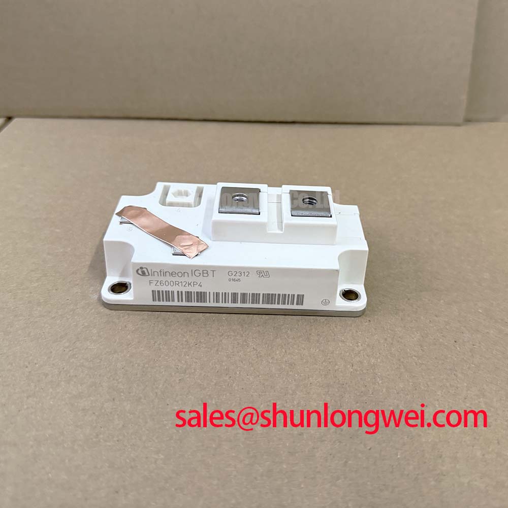
Operating high-capacity central solar inverters rated for megawatt-scale grid feed-in places immense dynamic stress on medium-voltage power stages. The FZ600R12KE3_B1 is a single-switch half-bridge building block rated at a collector-emitter breakdown voltage of VCES = 1200 V (Official Datasheet Specification) with a continuous collector current capability of IC = 600 A at a case temperature of TC = 80°C (Official Datasheet Specification). In 1500V DC-bus solar topologies—commonly arranged in three-level Neutral Point Clamped (NPC or A-NPC) converter architectures—rapid switching transients subject the gate loop to steep voltage and current gradients.
When switching current loads up to the repetitive peak rating of ICRM = 1200 A (Official Datasheet Specification), stray inductance inside the power emitter path interacts with steep di/dt transitions. If the gate driver reference is tied directly to the main power terminal, the voltage drop induced across the internal emitter busbar couples directly into the gate-emitter circuit. This feedback mechanism causes gate chatter, false turn-off commands, or parasitic re-turn-on due to Miller capacitance displacement currents. To eliminate this mutual coupling, the physical drive layout must strictly separate the auxiliary Kelvin emitter terminal from the main output power return.
💡 Pro Tip: Always run the auxiliary Kelvin emitter trace and the gate signal as a tightly coupled, balanced differential pair or twisted wiring harness directly from the driver stage to the module pins. Keep this path completely isolated from high-current DC-link return planes. Inserting a negative gate bias between -5 V and -15 V during the turn-off hold state provides essential noise immunity against ground bounce, well within the absolute maximum gate-emitter rating of VGES = ±20 V (Official Datasheet Specification).
During preventative maintenance inspections of central inverter power blocks, verify the integrity of the gate-emitter drive wiring. Measure the dynamic gate-source waveforms under load using high-voltage differential probes. Look for high-frequency ringing exceeding the threshold window of VGE(th) = 5.0 V to 6.5 V (Official Datasheet Specification). Excessive ringing during commutations indicates mechanical loosening of terminal connections, degraded gate damping resistors, or localized inductive coupling across the driver interface.
Transient Thermal Impedance (Zth(j-c)) & Multi-Layer Foster/Cauer Modeling
Thermal management dictates the long-term operational boundary of central solar stations subjected to diurnal load profiles. Daily cycles span zero-current standby at dawn to maximum current injection during peak solar irradiance. Under nominal conduction, the module exhibits a typical saturation voltage of VCE(sat) = 1.70 V at IC = 600 A and Tvj = 25°C (Official Datasheet Specification). Dissipating the resulting steady-state and switching losses demands precise modeling of the transient thermal path from the silicon junctions to the ambient exhaust stream.
The junction-to-case thermal resistance for the IGBT switch is specified at Rth(j-c) = 0.040 K/W (Official Datasheet Specification). In operational simulation and dynamic thermal load budgeting, a multi-stage Foster or Cauer equivalent RC network represents the thermal mass of the silicon chip, the direct copper bonded (DCB) ceramic substrate, the copper baseplate, and the thermal interface material (TIM). Under short-duration overload events—such as low-voltage ride-through (LVRT) reactive power support—the thermal capacitance of the silicon chip dominates heat absorption over the initial milliseconds, preventing instantaneous overtemperature before heat reaches the liquid cold plate or forced-air heatsink.
| Parameter | Symbol | Official Datasheet Value | Test Conditions |
|---|---|---|---|
| Collector-Emitter Breakdown Voltage | VCES | 1200 V | Tvj = 25°C |
| Continuous DC Collector Current | IC | 600 A | TC = 80°C, Tvj max = 150°C |
| Repetitive Peak Collector Current | ICRM | 1200 A | tp = 1 ms |
| Collector-Emitter Saturation Voltage | VCE(sat) | 1.70 V (typ.) | IC = 600 A, VGE = 15 V, Tvj = 25°C |
| Thermal Resistance, Junction-to-Case | Rth(j-c) | 0.040 K/W | per IGBT, Official Datasheet Specification |
| Maximum Operating Junction Temperature | Tvj op | -40°C to +150°C | Continuous operation under load |
Maintaining junction temperatures within the rated operating envelope of Tvj op = -40°C to +150°C (Official Datasheet Specification) requires balancing inverter carrier frequency against cooling capacity. Operating between 2.5 kHz and 4.0 kHz represents a balanced starting point for high-power utility inverters, keeping combined conduction and switching losses within manageable dissipation limits without inducing thermal runaway at elevated ambient temperatures.
When comparing power density upgrades or evaluating successor designs, engineers often reference the FZ600R12KE4, which incorporates updated trench-field-stop silicon technology. However, maintaining the installed base of third-generation modules requires strict maintenance protocols focused on interface thermal resistance.
⚠️ Maintenance Note: Thermal grease degradation is a primary failure mode in field-deployed inverters. Over continuous multi-year operation, thermal paste undergoes matrix pump-out and dry-out cycles caused by baseplate thermal flexing. During scheduled maintenance overhauls, inspect the baseplate-to-heatsink boundary. Reapply a uniform 50 µm to 100 µm layer of high-conductivity paste, and torque the M6 baseplate mounting screws incrementally to 3.0–6.0 N·m (General Industry Design Consideration for standard module baseplate mounting) to guarantee low thermal contact impedance across the entire DCB footprint.
Atmospheric Neutron Radiation Impact on 1200V/1700V Silicon Reliability
Utility-scale solar installations are frequently constructed in high-altitude desert plateaus above 2000 meters to maximize solar yield. At these elevations, the atmospheric shielding against cosmic radiation is significantly reduced, leading to an elevated flux of high-energy terrestrial neutrons. When an energetic neutron collides with the silicon crystal lattice inside the high-electric-field depletion region of a blocked IGBT, localized nuclear interactions can generate secondary ion tracks. This creates a highly conductive plasma filament that triggers catastrophic Single Event Burnout (SEB).
Because cosmic-ray-induced SEB occurs spontaneously without prior junction degradation, mitigating failure rates relies on DC-bus voltage derating rather than operational temperature management. While the FZ600R12KE3_B1 provides a rated blocking capability of VCES = 1200 V (Official Datasheet Specification), running the device continuously at high stationary DC voltages substantially increases the Failure In Time (FIT) rate at high altitudes.
In three-level 1500V DC central solar converter topologies, the stationary DC voltage across each individual 1200V IGBT switch is typically constrained to half the total bus voltage—between 750 V and 850 V. Maintaining this operational headroom provides essential protection against neutron-induced breakdown. Field engineers must factor altitude derating profiles into their system safety margins. Detailed methodologies for field-stress qualification and systematic semiconductor analysis are outlined in the Field Engineer’s Handbook.
For modular converter designs and sub-assembly planning, referencing the comprehensive Infineon IGBT Modules Overview provides structural insight into standard housing platforms and voltage class allocations across various industrial conversion domains.
Fault-Clearing Dynamics: Type-I/II Desaturation Detection and Inductive Clamping
Grid-tied central solar inverters face severe fault conditions, including line-to-line output short circuits, ground faults, and transformer saturation events. The FZ600R12KE3_B1 is engineered to withstand short-circuit conditions within the strict boundaries of its Short-Circuit Safe Operating Area (SCSOA). The gate driver circuitry must detect and fully interrupt fault currents within a maximum clearing duration of 10 µs.
Short-circuit events in power conversion are categorized into two primary mechanisms:
- Type-I Short Circuit: The IGBT turns on directly into an existing low-impedance short circuit. The rate of current rise is governed primarily by stray loop inductance, with the collector voltage remaining clamped at the full DC-bus potential.
- Type-II Short Circuit: A short circuit occurs while the IGBT is already fully turned on and conducting nominal load current. The collector-emitter voltage rapidly desaturates out of the low-loss conduction state, driving the silicon die into its active saturation region under full bus voltage stress.
To protect against Type-II desaturation, the driver circuit monitors VCE via a high-voltage sensing diode during the conduction cycle. When the collector-emitter voltage exceeds a preset desaturation threshold (typically 6.5 V to 8.0 V after a 2.0 µs to 3.5 µs blanking filter time), the driver initiates an immediate fault-clearing sequence. Standard hard turn-off during an active short-circuit event must be avoided; the rapid reduction of fault currents reaching several thousand amperes across parasitic busbar inductance produces catastrophic overvoltage spikes that can instantly exceed the 1200 V breakdown threshold.
Implementing Two-Stage Soft Turn-Off (2SSTO) or active collector-gate clamping mitigates this risk. During a desaturation trip, the driver reduces the gate voltage to an intermediate level before fully pulling down the gate, controlling the di/dt slope and safely dissipating the stored inductive energy. For auxiliary power rails and smaller distributed subsystems within the balance-of-plant, engineers often evaluate integrated platforms such as Infineon CIPOS™ Intelligent Power Modules (IPM), which feature onboard gate drive and protection circuits.
⚠️ Field Alert: During inverter commissioning and post-event troubleshooting, always verify the clamping voltage levels across the main DC busbars. Check that local high-frequency snubber film capacitors are mounted directly across the module's DC terminals. Loose snubber hardware increases parasitic loop inductance, compromising the soft turn-off safety margin and exposing the silicon to destructive voltage transients during emergency grid disconnects.