

Content last revised on September 12, 2026
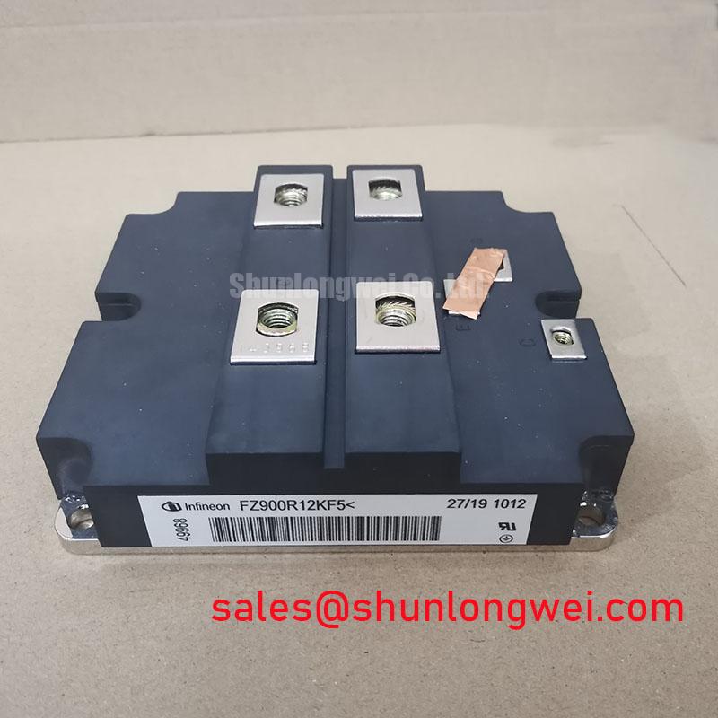
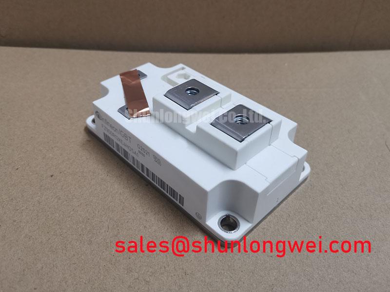
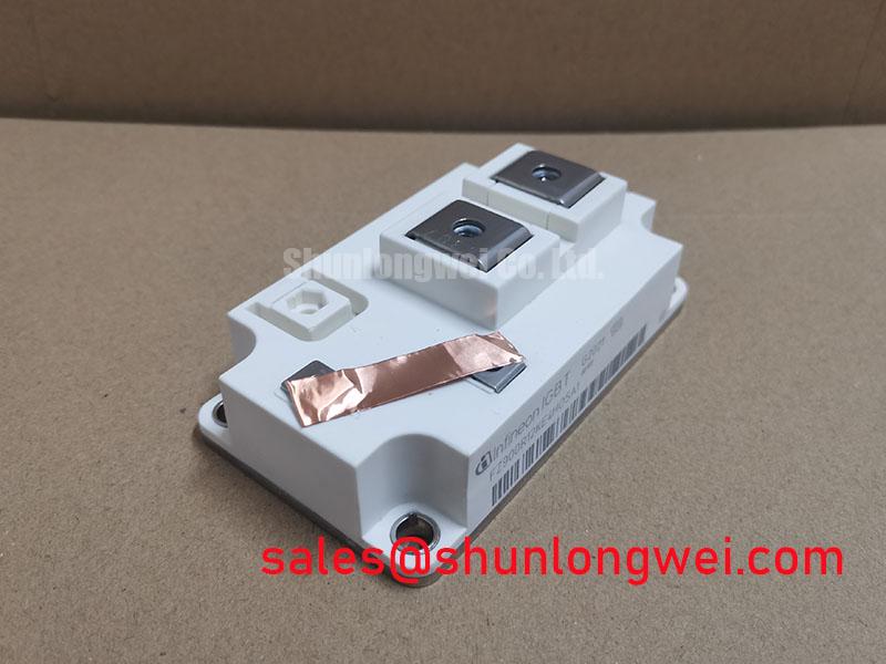
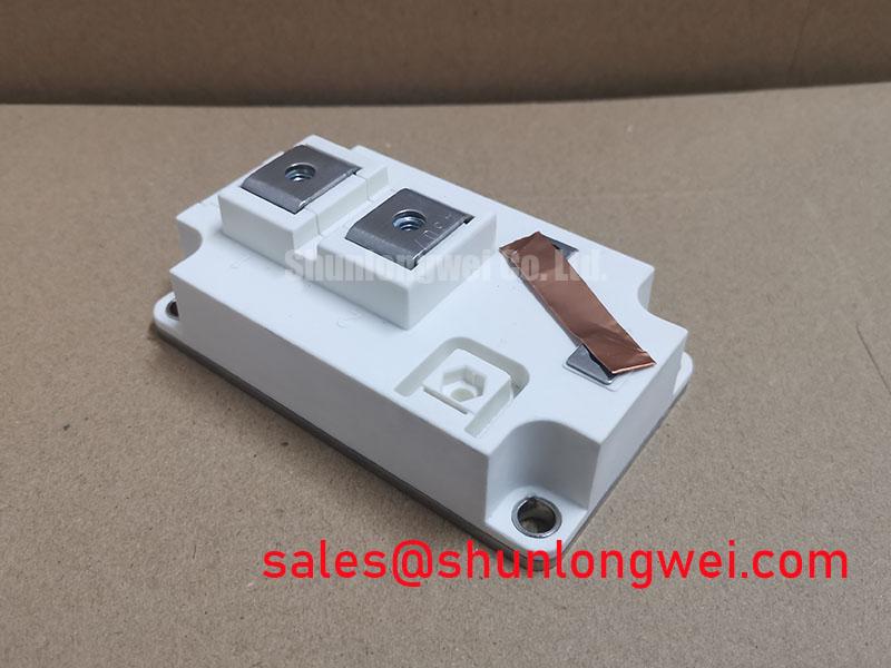
FZ900R12KE4HOSA1 Circuit Protection and Reliability in High Frequency Commutation Loops
During a field replacement, confirm that the DC bus, phase output, gate terminals, and auxiliary connections match the original wiring before energising the converter. A 1200 V rating does not by itself confirm suitability for every 1500 V photovoltaic inverter topology. System voltage, series connection, clamping arrangement, switching waveform, insulation coordination, and transient margin remain system-level design conditions.
When the switch turns off, stray inductance in the commutation path can convert changing current into an additional collector-emitter voltage. The practical relationship is that the peak voltage rises with both loop inductance and current slew rate, so the system designer should minimise the high-current loop area and verify the measured peak against the module’s permitted switching conditions. The target inductance, snubber value, and clamp voltage must be determined from the actual bus structure and switching test data rather than copied as universal values.
For a central solar inverter, inspect the laminated or planar busbar transition from the DC-link capacitor to the power module. Keep the positive and negative current paths closely coupled, maintain consistent phase geometry, and avoid routing gate-drive conductors through the high di/dt power corridor. Clearance and creepage should be selected from the working voltage, pollution environment, altitude, insulation system, and applicable equipment standard. The Infineon IGBT Modules and Discretes Official Portfolio provides the appropriate manufacturer-level reference point for product-family and application documentation.
In troubleshooting, use a differential high-voltage probe and a current probe at the same switching event. Compare turn-off overshoot, ringing frequency, gate-emitter disturbance, and diode commutation behaviour against a known-good phase. If a snubber or active clamp is fitted, check its physical loop, capacitor condition, resistor heating, and connection torque. A damaged clamp can leave the module apparently functional during low-power testing while allowing excessive transient stress at rated operating conditions.
The front end of a converter may include a separate rectifier or controlled conversion stage. In a system topology review, engineers can assess the related FZ800R12KS4_B2 as a neutral reference for an associated power stage, without treating it as an automatic substitute or confirmed companion device.
Field Diagnostics and Commissioning for Hard Switching Transients
Before commissioning, discharge the DC link using the equipment manufacturer’s approved procedure and verify the absence of hazardous voltage with a suitable meter. Inspect terminal plating, busbar contact faces, gate-drive connectors, insulating supports, and signs of localised heating. Cold resistance checks can identify an obvious short or open condition, but they cannot prove dynamic switching health, insulation integrity, or gate oxide condition.
Short-circuit protection must be evaluated as a complete control function. The gate driver, desaturation or current-sensing circuit, blanking behaviour, fault latch, isolation barrier, and turn-off profile all influence the stress seen by the FZ900R12KE4HOSA1. The exact short-circuit withstand time and SCSOA boundary are official datasheet matters and should not be inferred from the general 1200 V or 900 A ratings. Designers should validate the complete protection response with controlled tests at the intended bus voltage, temperature, gate resistance, and load configuration.
A two-stage soft turn-off strategy can reduce the voltage excursion associated with an abrupt interruption, but its timing and gate-current profile are system-dependent. The first action should remove the drive energy in a controlled manner; the second should establish the off-state while the protection circuit confirms that the fault is contained. The gate driver must also prevent complementary devices from receiving overlapping commands. Dead time should be selected from measured turn-off delay, propagation variation, device temperature, diode recovery, and the required output waveform. It should then be verified on the actual gate-emitter and collector-emitter waveforms rather than accepted from a nominal controller setting.
Pay attention to common-mode ground bounce. A long return conductor shared by the power emitter path and the driver reference can create a false gate signal during high-current commutation. Use a compact, symmetrical gate loop, separate power and signal returns where the module and driver architecture permit, and shield sensitive control wiring from the switching node. A negative off-state bias may be considered only when it is supported by the selected driver, isolation design, and the manufacturer’s gate-emitter limits. The required value is not established by the module’s headline voltage and current ratings.
After the first low-energy pulse test, compare all parallel phase legs for gate amplitude, turn-on delay, turn-off delay, collector-emitter overshoot, and current rise. A mismatch may indicate layout asymmetry, driver variation, probe placement error, or a power-path problem. Confirm the measurement setup before replacing the module.
Transient Dynamics, Derating, and Parameter Matching
The 900.0 A current figure is an official rating, not a guaranteed operating current under every cooling arrangement, switching frequency, pulse duration, or case temperature. Continuous current capability is governed by junction temperature, case temperature, thermal impedance, conduction loss, switching loss, busbar design, and the protection settings of the complete inverter. For a utility-scale 1500 V central photovoltaic inverter, the system integrator must first establish how the 1200 V device rating fits within the actual electrical topology and transient protection scheme.
When multiple modules operate in parallel, the positive temperature coefficient commonly associated with IGBT conduction voltage can support static current sharing as temperature changes. This remains a design consideration, not a substitute for measurement. Dynamic current sharing is affected by gate-loop inductance, emitter-path impedance, driver timing, stray capacitance, diode recovery, and the position of the current sensor. Match the physical gate-drive paths, use equivalent power-path geometry, and verify current balance during both turn-on and turn-off.
Do not use a single multimeter voltage reading as proof that parallel devices share correctly. Capture the switching current in each branch, then compare the waveform at the intended operating temperature and load. If one branch rings or carries a disproportionate pulse, inspect busbar symmetry, gate resistor placement, mounting contact, driver isolation, and probe loop area before changing control parameters.
Free-wheeling diode behaviour also affects the next IGBT turn-on event. Reverse recovery charge, recovery softness, commutation inductance, and the resulting electromagnetic field can change both device stress and conducted or radiated interference. The recovery softness factor, often represented by a manufacturer-defined parameter, must be taken from the relevant diode data rather than assumed from the IGBT current rating. EMC compliance belongs to the assembled inverter and its installation; the module itself should not be described as independently certified to an equipment-level CISPR or EN 55011 limit.
Some converter architectures place controlled rectifiers or thyristors ahead of the inverter bridge. Their gate trigger current and gate trigger voltage are separate device-specific parameters and should be checked from the relevant thyristor documentation. A strong trigger pulse train can improve immunity to noise in some control schemes, but pulse width, repetition, isolation, and thermal conditions must be validated by the system designer.
For neutral cross-reference work, engineers may review FZ3600R12HP4 as another Infineon high-power module listing. Package geometry, electrical topology, gate requirements, internal diode arrangement, and mechanical interfaces must be compared directly before any replacement decision.
FZ900R12KE4HOSA1 Thermal and Electrical Optimisation
Remove old interface material completely and inspect the cooler for flatness, contamination, burrs, and local distortion before installing the replacement module. The thermal interface layer should be continuous and thin enough to avoid unnecessary thermal resistance, while still filling the microscopic surface irregularities. A common engineering starting range for a spread thermal compound layer is approximately 50 to 100 µm, but the compound supplier, cooler finish, baseplate condition, and assembly process determine the acceptable result.
Apply the compound evenly across the intended contact area and avoid trapped air pockets. Excess material can migrate toward insulation surfaces or fasteners; insufficient material can leave dry contact zones. If the module baseplate or heatsink shows curvature, do not compensate by forcing one corner down. Correct the mechanical condition or use an approved interface and mounting method that maintains uniform contact.
Mounting should follow a crosswise, progressive sequence so the baseplate settles evenly. The final torque is a mechanical design consideration determined by the fastener size, thread condition, washer arrangement, module construction, and manufacturer instructions. After tightening, inspect for baseplate movement, displaced compound, tilted hardware, and stressed terminals. Recheck the power connections after the first controlled thermal cycle according to the equipment service procedure.
⚠️ Field Alert: Disconnect and verify the DC link is discharged before inserting or removing gate-drive connectors, and use the approved module mounting torque rather than relying on hand feel.
Thermal commissioning should record case temperature, coolant or heatsink conditions, phase current, switching frequency, gate waveform, and protection events together. A rising temperature trend can involve interface resistance, airflow, coolant performance, current imbalance, excessive switching loss, or an inaccurate sensor position. Compare the complete thermal-electrical record with the equipment limits and the applicable Infineon documentation.
For a broader discussion of switching behaviour and industrial drive design, engineers can consult Unlocking Efficiency in Industrial Drives. It should be used as an engineering reference alongside the exact product datasheet, gate-driver documentation, inverter schematic, and measured commissioning data.