Content last revised on October 7, 2026
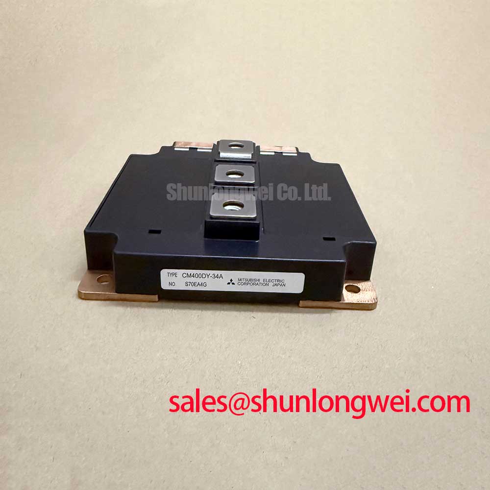
CM400DY-50H Initial Replacement Checks
With the inverter isolated and its DC link confirmed discharged, compare the installed module’s terminal layout and nameplate with the replacement documentation before loosening the busbars. CM400DY-50H is a Mitsubishi Electric IGBT module with an official rated voltage of 2500 V and rated current of 400 A. Those ratings establish initial electrical boundaries; they do not, by themselves, establish suitability for a utility-scale 1500 V central solar inverter.
Evaluating Thermal Capacitance vs Heat Sink Time Constant under Surge Bursts
A short overload and a sustained overload can produce different junction temperatures even when the measured current peaks are alike. During a surge burst, heat first accumulates close to the semiconductor junction. The case and heat sink respond later. For the CM400DY-50H, the 400 A rating is an Official Specification, not a permissible repetitive surge current or a substitute for a transient thermal impedance curve.
For a repair assessment, capture the actual current waveform and switching conditions, then check them against the Mitsubishi Electric documentation for the installed module. A multi-RC thermal model can estimate peak junction temperature from the time history of calculated device losses, but it needs the appropriate manufacturer thermal data and a measured or justified case-temperature boundary. Without those inputs, a numerical peak junction-temperature margin would be an assumption rather than an Engineering Calculation.
Inspect the cooling path while the assembly is accessible: look for uneven contact marks, obstructed airflow or coolant flow, and changes in case-temperature readings between comparable operating points. These observations do not identify a single fault on their own. They help determine whether the heat sink is removing energy between bursts or whether successive bursts may be raising the starting temperature. In a grid-tied solar inverter, that assessment should use the equipment’s measured operating cycle rather than an assumed constant load.
Selection also requires more than matching current. The linked CM400HA-12E can serve as a comparison point for documentation review, but its voltage class, internal circuit, terminal arrangement, thermal characteristics, and mechanical fit must each be checked against the original design. A shared current figure would not make two modules interchangeable.
Reinforced Insulation Barrier Integrity and Parasitic Coupling Capacitance Reduction
Before connecting a replacement gate driver, trace the isolation boundary on the equipment schematic and identify which insulation functions belong to the driver supply, signal isolator, board layout, and module mounting system. The supplied CM400DY-50H product data confirms its 2500 V rated voltage and 400 A rated current; it does not establish a reinforced-insulation rating or a common-mode transient immunity value. Both require verification from the documentation for the relevant parts and the complete assembly.
Parasitic capacitance across an isolation boundary can transfer common-mode current during fast switching. As a Design Consideration, keep the gate-drive return path controlled and inspect clearance around high-voltage conductors, isolated supplies, connectors, and mounting hardware against the equipment’s approved drawings. Clearance and insulation decisions must reflect the actual installation conditions and applicable system requirements, rather than a spacing rule inferred from the module’s voltage rating.
Gate-drive source and sink capability and the external gate resistor should be evaluated together. More drive current can change switching transitions, while resistor selection influences ringing, losses, and the gate voltage seen during the opposite switch’s transition. Measure the waveforms at the module terminals under controlled test conditions; use the driver and module manufacturers’ documented limits to judge the result. If an isolation concern is suspected, the Field Engineer’s Handbook provides a broader framework for organizing measurements and failure analysis, but it does not replace the applicable insulation specifications.
Suppressing C_res Induced Gate Voltage Spikes in High-Voltage Inverter Bridges
When one bridge position switches, collector-to-gate coupling can disturb the gate voltage of the device that should remain off. This coupling is often described in terms of reverse-transfer capacitance, or C_res. A gate trace that appears quiet at the driver output may still show a spike at the module connection, so compare measurements at both locations using a probe arrangement suitable for the circuit’s voltage and switching environment.
For the CM400DY-50H, do not assume that an auxiliary emitter connection or a particular gate-drive topology is present without checking the official terminal diagram. If the equipment provides a separate gate-return path, route and assess it according to that diagram. An active Miller clamp or negative off-state bias may be evaluated as a system-level mitigation, but neither a clamp threshold nor a bias setting can be prescribed from the supplied module ratings alone. The driver specification, measured gate waveform, switching loss, and fault-response behavior determine what the system can accept.
💡 Pro Tip: Measure the off-state gate voltage at the module during the opposite device’s switching transition before changing the gate resistor, because a driver-board reading can miss local ringing.
Keep the power commutation path and gate-drive path distinct in the layout review. Stray inductance and rapid current change can raise switching overshoot, so verify measured collector-emitter peaks against the module’s 2500 V Official Specification under the inverter’s relevant operating conditions. Magnetic-field forces are a separate mechanical concern in high-current conductors; the Maxwell stress tensor explains the underlying field mechanics, but it supplies neither a busbar support specification nor a qualification result for this module.
Thermal Interface Material (TIM) Thickness Uniformity and Void Minimization
Remove the module with attention to the existing contact pattern. Concentrated paste at one edge, broad dry regions, or localized impressions can indicate that the interface needs investigation, though none proves the cause of a thermal problem by itself. Clean the mating surfaces using a process compatible with the materials, and inspect the heat sink and module mounting faces before applying the approved thermal interface material.
Apply the interface material to promote continuous contact without using an assumed universal film thickness. The supplied CM400DY-50H parameters do not specify a TIM thickness, allowable baseplate curvature, or mounting torque. As a Design Consideration, follow the applicable Mitsubishi Electric mounting instructions and the equipment manufacturer’s heat-sink procedure; tighten the fasteners in the documented sequence so the interface is compressed evenly. The final method must account for the actual module, fasteners, heat sink, and TIM.
After reassembly, compare case-temperature measurements at repeatable load conditions and inspect the resulting temperature spread before returning the inverter to its normal operating cycle. If a hot spot remains, check the cooling path, sensor placement, mounting contact, and electrical loading together rather than assigning the temperature rise to the TIM alone.