

Content last revised on September 24, 2026
Transient Dynamics & Electrical Design: High Frequency Commutation Loop Inductance on CM400DY-34A
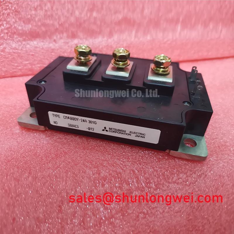
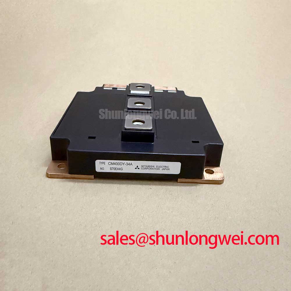
Before energizing a test fixture, isolate the CM400DY-34A, inspect its module case and terminals, then verify the marked power and gate connections against the applicable Mitsubishi Electric documentation. The published product data identifies this Mitsubishi Electric unit as an IGBT Module with a rated voltage of 1700.0 V and a rated current of 400.0 A. The specified package is Module. These are official product parameters supplied for identification and initial system compatibility review; switching frequency, gate limits, thermal impedance, terminal arrangement, isolation rating, and transient limits should be confirmed from the correct device datasheet before applying power.
For incoming inspection, use an ESD controlled bench and begin with a visual examination of the molded case, mounting surfaces, power terminals, control terminals, and labeling. A cold resistance comparison between corresponding terminals can help identify an obvious short or open condition, but a resistance reading alone does not establish semiconductor health. A diode test may show a forward conduction path through an antiparallel diode, depending on the accessible terminal pair and the meter polarity. Record the test polarity and compare the result with a known good reference or the manufacturer’s terminal diagram rather than assigning a universal “normal” voltage window.
💡 Bench Tip: Keep the module discharged and disconnected from the gate driver before measuring terminals, and record the cold reference readings before any high voltage test.
In a high voltage converter, the first design task is to identify the complete commutation loop around the 1700.0 V module rating, DC link, switching device, freewheel path, and local capacitor network. Stray loop inductance converts rapid current change into voltage overshoot, so the practical objective is to minimize the physical loop area and keep the high current path short, broad, and symmetrical. The relationship can be evaluated during switching tests using the principle that the inductive overshoot increases with loop inductance and current slew rate. The system engineer must measure the actual peak voltage and verify that it remains within the selected operating boundary.
The supplied application outline refers to a sub 25 nH layout target. That value should be treated as a system engineering target for the proposed busbar architecture, not as an official electrical specification of the CM400DY-34A. A laminated or planar busbar arrangement may reduce the opposing current path area, but the final result depends on the complete converter geometry, capacitor placement, fastening method, and measurement technique. Use a properly rated differential probe with a short connection arrangement when examining turn off voltage. Long probe leads can create ringing that is not representative of the module terminals.
Snubber selection also requires measured switching data. A capacitor that is too small may leave excessive overshoot, while an unnecessarily large capacitor can increase switching loss and alter turn on behavior. Designers should evaluate the capacitor, damping resistance, pulse current, dielectric voltage rating, and thermal dissipation as one network. If a battery energy storage PCS exhibits a repetitive gate fault or unexplained DC link trip, compare the collector emitter waveform, gate emitter waveform, and driver supply at the module pins. A discrepancy between the driver output and the module gate terminal may indicate layout coupling, common impedance, or probe reference problems rather than an intrinsic module failure.
When selecting associated power devices, the CM50DY-28H may be reviewed as a related component in a broader rectifier or front end topology. It is not a substitute recommendation for the CM400DY-34A. The system designer should confirm voltage class, current duty, topology position, control timing, and thermal conditions independently.
Assembly Integrity & Layout Architecture: Implementing Multi Module Parallel Current Sharing for CM400DY-34A
Parallel operation requires more than matching the nominal current rating. The current path from the DC bus to each module must have comparable impedance, busbar length, contact quality, and thermal environment. A positive temperature coefficient of on state voltage can support static current sharing in some IGBT operating regions, but the actual balance remains dependent on gate timing, junction temperature, stray inductance, and device characteristics. This behavior should be verified through measured current sharing under the intended load profile rather than assumed from the 400.0 A nameplate rating.
Begin assembly by confirming the terminal drawing for the exact production variant. Do not infer the power, gate, auxiliary, or emitter connections from a visually similar module. Use continuity checks only with the device isolated from the driver and DC link. For a parallel bank, route each gate loop with comparable length and return geometry. The driver output should reach each module with controlled impedance, while the power return should not share a narrow PCB trace with the gate return.
Mechanical flatness and contact pressure affect thermal transfer and electrical repeatability. Apply the selected thermal interface material as a controlled, uniform layer suitable for the module baseplate and heatsink surfaces. The correct compound, coverage, curing behavior, and application thickness must come from the thermal interface supplier and equipment design. Mounting torque must likewise follow the module drawing and hardware specification; do not transfer a generic torque value to this product without confirmation.
Clearance and creepage must be checked across the actual busbar, insulation, fasteners, and contamination environment. The 1700.0 V rating does not by itself define the required spacing for a finished PCS assembly. Designers should evaluate working voltage, pollution conditions, altitude, insulation material, and applicable equipment standards. During service, inspect for loose busbar joints, discoloration, uneven contact marks, and signs of local heating. These observations can guide further testing but should not be treated as proof of a single failure mechanism.
For a neutral comparison during replacement assessment, engineers may review FF45017ME4 as another Mitsubishi Electric high power module listing. Electrical interchangeability is not established by package appearance or current rating alone. Gate requirements, internal topology, terminal spacing, switching characteristics, and thermal data must all be matched against the original design.
Preventing Spurious Faults: PCB Symmetry Considerations for Dual IGBT Guidelines for CM400DY-34A
A dual IGBT module can be sensitive to the way the control return is connected to the high current emitter path. When the gate driver return shares impedance with a pulsed power emitter conductor, the resulting voltage movement can appear at the gate and create unwanted turn on, ringing, or protection activation. The layout principle is to keep the control return path separate from the high current path for as far as the module terminal arrangement permits. Whether an auxiliary emitter connection is available on the exact device version must be confirmed from the terminal drawing rather than assumed.
Dead time should be established from measured turn off and turn on behavior, driver propagation delay, temperature, load current, and the reverse recovery behavior of the associated diode path. Excessive dead time can increase conduction loss, while insufficient dead time can create cross conduction. A bootstrap supply, if used by the system architecture, must be checked for capacitor recharge, driver quiescent current, duty cycle, diode recovery, and voltage droop. These are system design conditions, not published CM400DY-34A product parameters.
Desaturation protection and soft shutdown should be evaluated with the actual driver board. The protection circuit must distinguish a genuine overcurrent event from switching noise and should limit the gate transition in a controlled manner during a fault. The short circuit safe operating area, gate voltage limits, fault response time, and repetitive fault capability require the applicable Mitsubishi Electric device and driver documentation. Do not assign a microsecond protection value to this module without a verified source.
For reference, Mitsubishi Electric’s Power Semiconductors & High Power Modules and Global Semiconductor Device Technologies provide manufacturer level information. These resources can help establish the correct documentation path, while the final PCB must still be validated with oscilloscope measurements at the module terminals.
Benchtop Waveform Tuning: Mitigating Stress via Evaluating Thermal Capacitance vs Heat Sin on CM400DY-34A
Thermal evaluation should start with the real pulse profile rather than the nominal current number. A 400.0 A rating does not automatically represent continuous operation under every switching frequency, case temperature, duty cycle, or cooling arrangement. For a battery PCS, capture the collector emitter voltage, gate emitter voltage, current waveform, case temperature, heatsink temperature, and relevant driver supply during representative charge and discharge transitions.
A transient thermal network can be used to estimate junction temperature from measured power pulses. In practical terms, the engineer calculates the energy dissipated during each switching and conduction interval, applies the manufacturer’s junction to case and case to heatsink thermal data, and then checks the resulting temperature rise against the permitted operating conditions. The thermal capacitance of the assembly influences short pulses, while the heatsink and coolant path dominate longer load intervals. The required thermal parameters must come from the official device documentation and the completed mechanical assembly.
Waveform tuning should compare switching loss against voltage overshoot and electromagnetic disturbance. Slowing the gate transition may reduce ringing but can increase switching dissipation. Increasing gate resistance may produce a different result at hot and cold conditions, so bench tests should cover the intended operating envelope. If a waveform shows unexpected oscillation, first verify probe grounding, current sensor bandwidth, gate loop routing, DC link capacitor position, and mechanical connections before attributing the behavior to the IGBT die.
Insulation and withstand testing require a controlled procedure appropriate for the finished PCS. Confirm the module’s specified isolation information, test voltage, duration, ramp method, and discharge process from the correct documentation. The Field Engineer’s Handbook can be used as a practical reference for structured inspection and measurement planning. It does not replace the manufacturer’s limits or the safety procedures applicable to the energized equipment.
Before approving the CM400DY-34A for a replacement or new design, the integrator should reconcile the official 1700.0 V voltage class, 400.0 A current rating, module package, terminal configuration, gate driver behavior, cooling method, insulation design, and measured switching waveforms with the original PCS requirements.