

Content last revised on September 27, 2026
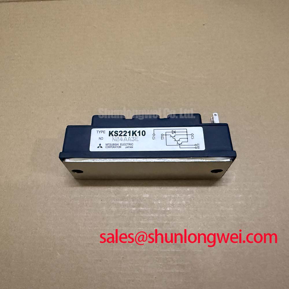
Verify the nameplate ratings, inspect the power terminals and housing, then perform a controlled cold-state resistance check before connecting KS221K10 to an energized converter. The Mitsubishi Electric unit is specified for a repetitive peak off-state or reverse voltage of up to 1800 V, an average on-state current of 220 A, an RMS on-state current of 345 A, and a peak one-cycle surge current of 5500 A. Its specified critical off-state voltage rise capability is 1000 V/µs, with an isolation voltage of 2500 Vrms. These are official product specifications supplied for engineering evaluation; the complete equipment ratings remain system-dependent.
KS221K10 Thermal-Electrical Optimization: Multi-Module Parallel Current Sharing Practical Tuning
When several power modules are connected in parallel, current sharing should be checked in both steady-state operation and switching or commutation operation. The temperature dependence of the device on-state voltage can influence static current balancing, but its effect depends on operating current and temperature. This is a design consideration rather than a substitute for measured sharing data. Differences in busbar resistance, terminal pressure, trigger-loop impedance and thermal contact can still produce unequal current distribution.
For a commercial string inverter or micro-grid energy storage converter, begin with a symmetrical physical arrangement. Keep the DC positive and negative paths geometrically similar for each parallel branch, and route the trigger or firing conductors with comparable length and return geometry. The control board should not rely on one branch carrying the entire switching reference for the others. Each trigger path should be reviewed for its own gate-cathode reference, pulse characteristics and local noise environment, subject to the actual terminal configuration documented for the device.
Dynamic balance is often more sensitive than static balance. A branch that turns on slightly earlier can momentarily take a disproportionate share of current, while a branch that turns off later during circuit commutation can experience additional stress. Review trigger-pulse timing, trigger-source impedance and the mutual coupling between power and control conductors as a complete network. Rapid anode-voltage changes can interact with device capacitances and wiring to produce unwanted gate-cathode disturbance or false triggering. A suitable snubber, gate-cathode network or other suppression method may be evaluated where the switching waveform shows unwanted triggering, but the final protection values must be established from the trigger-circuit design and measured transient behavior.
Thermal verification should use temperature measurements from comparable locations on every parallel branch. A branch with better cooling can carry more current without immediately showing a high case temperature, while a branch with poor interface contact may show the opposite pattern. Compare anode-cathode voltage, gate-cathode voltage, trigger timing and commutation timing at the same operating point. If one waveform differs, inspect the complete trigger loop and busbar path before assigning the result to the semiconductor itself.
The current and voltage ratings should be treated as device boundaries, not as a complete converter operating point. Engineers should verify conduction loss, commutation behavior, repetition rate, cooling performance, short-circuit protection and transient overshoot against the actual application. The three-phase power relationship and branch symmetry should also be reviewed using established system analysis methods such as Three-Phase Electric Power Balance and Symmetrical Components.
For a sourcing comparison, CM50DY-28H may be reviewed as a separate Mitsubishi Electric product record. It should not be treated as a direct replacement until voltage class, current definition, internal circuit arrangement, mechanical interface, isolation requirement and control-terminal compatibility have been checked against the original equipment documentation.
Transient Dynamics & Electrical Design: Isolated Trigger-Supply Sizing for KS221K10
The isolated trigger supply must be evaluated as part of the switching cell rather than as an independent accessory. Confirm the required output voltage, current, isolation construction, startup behavior and protection functions from the original trigger-circuit documentation. The supplied 2500 Vrms isolation rating is an official specification for the module; it does not establish the insulation coordination of the complete trigger power supply, PCB, connector system or enclosure.
Where the equipment specification calls for reinforced galvanic isolation or a high common-mode transient immunity target, the system integrator should verify those requirements against the isolated converter data sheet and the assembled trigger-circuit test results. A converter’s isolation rating and a trigger circuit’s transient immunity are different characteristics. The complete circuit should be tested with the actual switching voltage, trigger wiring, return path and mechanical spacing in place.
Trigger-loop inductance and wiring capacitance can convert a rapid anode-voltage transition into an unwanted gate-cathode disturbance. Keep the trigger-supply decoupling close to the trigger-current loop, separate high-current commutation paths from sensitive control traces, and use a defined gate-cathode return. Designers should minimize parasitic loop inductance where practical, then verify the peak gate-cathode and anode-cathode voltages with an oscilloscope during representative load and commutation tests. No fixed layout inductance or universal trigger-voltage value can be assigned to KS221K10 without the complete circuit topology.
Firing control requires an interlock and timing strategy appropriate to the converter topology and commutation method. The required pulse timing and any blanking interval are determined by trigger-circuit propagation delay, temperature variation, device turn-on behavior, load current, commutation path and measurement results. Treat these timing values as system parameters, not as assumed characteristics of the module. In a topology using complementary controlled devices, incorrect timing can increase conduction overlap, commutation stress or short-circuit risk.
During troubleshooting, compare the gate-cathode waveform at the module terminals rather than only at the trigger-circuit output. Check whether the reference node moves during the anode-voltage transition, whether the isolated supply droops during repetitive operation, and whether the trigger signal remains within the trigger circuit’s intended range. An abnormal trace may indicate coupling, inadequate decoupling, probing error, a damaged trigger circuit or an unsuitable return path; confirm the signal against a known-good channel before making a component-level judgment.
General information on Mitsubishi Electric power semiconductor technologies can be reviewed through the manufacturer’s CSTBT™ Technology resource. That reference should not be read as confirmation that every feature described there applies to this specific product record.
Assembly Integrity & Layout Architecture: Voltage Derating and Layout Guidance for KS221K10
High-voltage converter evaluation should start with the documented 1800 V maximum repetitive peak off-state or reverse voltage and the actual DC-link waveform. The voltage rating does not provide a universal altitude derating curve, cosmic-ray immunity guarantee or single-event burnout FIT value. Those subjects require manufacturer data, application qualification evidence or a project-specific reliability study. Without such a source, engineers should avoid assigning a numerical SEB probability or lifetime prediction to this component.
At elevated installation sites, environmental conditions can alter the system reliability assessment, but altitude alone does not establish a failure rate. The relevant review may include operating voltage, repetitive switching stress, transient overshoot, cooling conditions, insulation coordination, enclosure design and the statistical reliability model selected by the equipment manufacturer. Any voltage headroom decision should therefore be made by the system engineer after measuring the real DC bus and peak switching voltage under worst-case operating conditions.
Busbar architecture is a practical control point. Use compact, symmetrical laminated or closely coupled conductors where appropriate, and minimize the commutation loop area to reduce stray inductance. The turn-off or commutation transient is influenced by stray inductance and current slew rate, so the peak anode-cathode voltage must be measured directly at the module connection points. A voltage spike that is absent at the trigger-circuit test point may still exist at the power terminals.
Clearance and creepage must be established from the applicable insulation coordination requirements, pollution environment, working voltage, transient category and manufacturing tolerances. The module’s 2500 Vrms isolation specification should not be converted directly into a PCB spacing rule. Inspect the assembly for contamination, damaged insulation, sharp conductor edges and uneven terminal seating before high-voltage testing.
For field diagnosis, record the DC-link voltage, switching frequency, load current, ambient condition and heat-sink temperature together with the oscilloscope waveform. Compare the result with the equipment’s known-good baseline. A rising overshoot may reflect busbar geometry, trigger timing, commutation behavior, probe placement or load conditions; it should not be attributed to cosmic-ray exposure without supporting evidence. Thermal interface and cooling architecture can be reviewed alongside the technical background in The Advanced Thermal Management Revolution.
⚡ Safety Interlock Note: Discharge and verify the DC link before touching the module, trigger-circuit connector or oscilloscope probe, and follow the equipment manufacturer’s lockout procedure.
KS221K10 Circuit Protection & Reliability: Evaluating Thermal Capacitance Versus Heat Sink
The official current figures describe different operating conditions and should not be interchanged. The 220 A IT(AV) value is an average on-state current specification, the 345 A IT(RMS) value is an RMS on-state current specification, and the 5500 A ITSM value is a peak one-cycle surge current specification. The permitted use of each value depends on waveform, conduction angle, case temperature, cooling method, repetition and the manufacturer’s test conditions.
For pulsed overload evaluation, a thermal RC model can be used as an engineering calculation method. The model converts the measured or calculated power pulse into a junction-to-case temperature rise through the relevant transient thermal impedance. The peak junction temperature should then be checked against the applicable manufacturer thermal limits and the actual case-temperature measurement. A single steady-state thermal resistance value is not sufficient for short overloads because the heat flow evolves with time.
Heat-sink installation deserves the same attention as electrical layout. Confirm that the mounting surface is clean, flat and free from burrs, and apply the specified interface material according to the assembly documentation. If a clamp or pressure structure is used, calibrate the pressure distribution across the module rather than relying only on a fastener torque value. Uneven pressure can create localized thermal resistance and mechanical stress even when the average heat-sink temperature appears acceptable.
Double-sided cooling or other advanced thermal arrangements should be validated against the actual package construction and approved assembly method. Do not infer internal thermal paths, substrate materials or allowable clamping force from a different Mitsubishi Electric product. Where the original equipment uses a specialized pressure-contact arrangement, obtain its mechanical specification before replacing the power stage.
Protection coordination should include overcurrent detection, short-circuit response, firing inhibition, commutation behavior, DC-link discharge and fault recording. The module’s voltage and current ratings do not define the response time of the surrounding protection circuit. Engineers should verify that the measured fault waveform remains within the device and system boundaries during controlled testing, with the test method selected to avoid exposing personnel or equipment to uncontrolled stored energy.
When a converter shows a thermal imbalance, compare the heat-sink interface, busbar connection, trigger timing and current waveform across branches. A high case temperature may result from excessive conduction loss, commutation loss, poor thermal contact or inadequate airflow, while a lower measured case temperature does not by itself prove safe junction operation. Use synchronized electrical and thermal measurements to determine whether the issue is continuous, pulse-related or associated with a particular switching transition.