Content last revised on September 26, 2026
CM400DY-34TA Thermal Electrical Optimization and Gate Control
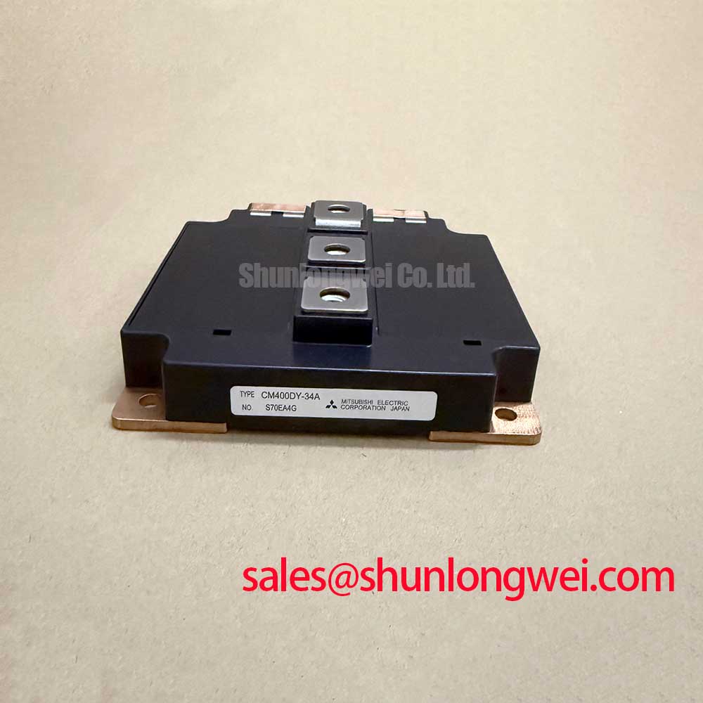
Begin incoming inspection by confirming the CM400DY-34TA marking, checking the power terminals for mechanical damage, and recording gate-to-emitter impedance and other appropriate cold-state checks before any powered test. Mitsubishi Electric identifies this device as a high-voltage IGBT module with an official collector-emitter voltage rating of 1700 V and a collector current rating of 400 A at Tc = 100°C. These limits must be checked against the converter’s measured DC-link voltage, switching current, cooling condition, and protection settings rather than treated as a complete system operating prescription.
The specified typical collector-emitter saturation voltage is 2.2 V at Tj = 25°C. This value is useful when estimating conduction loss and comparing the measured voltage waveform with a known-good phase leg. A field measurement should use the actual gate-drive timing, load current, junction temperature, and switching conditions. A higher observed value can involve gate-drive amplitude, temperature, current distribution, probe placement, or device condition, so the waveform should be reviewed with the complete switching sequence.
| Official parameter | Rated value | Engineering significance |
|---|---|---|
| Collector-emitter voltage, VCES | 1700 V | Defines the module’s stated blocking-voltage class for high-voltage converter evaluation. |
| Collector current, IC | 400 A at Tc = 100°C | Supports evaluation in high-current motor and power-conversion stages when thermal conditions are controlled. |
| Collector-emitter saturation voltage, VCE(sat) | 2.2 V typical at Tj = 25°C | Provides a reference for conduction-loss assessment at the stated test condition. |
| Isolation voltage, Visol | 4000 Vrms, AC for 1 minute | Defines the stated isolation withstand capability between the module terminals and its baseplate or case. |
| Thermal resistance, Rth(j-c) | 0.038 K/W for the IGBT part | Supports junction-to-case thermal calculations when the case temperature and mounting interface are known. |
High dv/dt can couple into an inactive gate loop and create unwanted gate movement. A Design Consideration is to keep the active gate-drive loop compact, route its return path with the corresponding drive conductor, and evaluate the turn-on and turn-off waveforms directly at the module terminals. Designers may assess an active Miller clamp or a negative gate-bias arrangement where the selected driver, isolation system, and module documentation support it. The final bias value remains system-determined and requires verification under the converter’s highest switching stress.
For a suspected cross-conduction event, first compare both complementary gate signals at the same time base, then inspect the collector-emitter voltage and phase-leg current. Look for timing overlap, abnormal gate ringing, driver supply disturbance, and common-source or emitter return inductance. This approach avoids assigning a single cause to a fault that may involve layout, driver isolation, control timing, or a damaged power path.
Preventing Spurious Faults in the Isolated Gate Power System
The isolated DC-DC supply should be evaluated as part of the gate-drive system, not as an independent accessory. Verify its required galvanic isolation against the converter’s insulation coordination requirements, including creepage, clearance, transformer construction, barrier testing, and transient behavior. The official module isolation rating is 4000 Vrms for one minute, but the complete gate-drive assembly must be assessed as a system because connectors, PCB contamination, heat sinks, mounting hardware, and cable routing can reduce practical isolation performance.
Common-mode transient immunity is also a system property. A driver that appears stable on a low-voltage bench may behave differently beside a fast-switching high-voltage bridge. As an Engineering Recommendation, evaluate the isolated supply and driver with the intended switching edge, gate-loop wiring, and DC-link arrangement. Use differential probes with suitable bandwidth and common-mode range, and compare the inactive gate terminal against its local emitter reference rather than against controller ground.
Dead-time should be established from measured device turn-off behavior, driver propagation delay, temperature variation, and the required control margin. The correct value is determined by the complete power stage, not by the CM400DY-34TA part number alone. Complementary gate interlock signals should be checked at the driver outputs and at the module terminals, since a clean controller waveform can be degraded by isolation delay, connector coupling, or an asymmetrical return path.
A practical incoming test sequence includes an unpowered continuity inspection, gate-to-emitter impedance comparison between channels, diode-mode checks across the module’s marked power paths where the terminal arrangement permits a meaningful reading, and a controlled insulation test performed with appropriate laboratory equipment. A diode-mode reading is a comparative screening result, not a substitute for the manufacturer’s dynamic diode data or a proof of switching health.
💡 Bench Tip: Use ESD controls and record a cold-state reference from a known-good unit before applying any gate-drive or insulation test voltage.
When the module is evaluated for a multi-megawatt offshore or onshore wind turbine full-scale converter, designers should also confirm the original converter’s gate-supply voltage, connector pinout, protection sequence, and discharge behavior from the equipment documentation. Do not assume compatibility from current and voltage ratings alone.
High-Frequency Commutation Loop Inductance and Overvoltage Control
Inspect the commutation path before changing snubber values. The physical loop includes the module terminals, DC-link capacitor connection, busbar geometry, laminated conductors, and any local suppression components. A wide, symmetrical current path with a short return path generally reduces parasitic inductance, but the final result must be confirmed by switching-waveform measurement. The switching overshoot follows the interaction between stray inductance, current slew rate, semiconductor behavior, and the available clamping network; the engineering relationship can be expressed in the familiar form that the inductive voltage contribution rises with Lσ multiplied by di/dt.
The layout target must be determined by the system engineer from the measured peak voltage and the module’s blocking-voltage boundary. It is not appropriate to assign a universal inductance limit without the converter topology, bus voltage, current waveform, switching speed, and clamp technology. Use a high-bandwidth measurement method with a very short probe connection, then compare turn-off peaks at different load currents and temperatures.
Snubber capacitors, resistive damping, and MOV networks should be coordinated rather than selected independently. The capacitor must withstand the repetitive pulse current and voltage stress, while the resistor controls the energy and ringing behavior of the local network. A MOV may help absorb slower or higher-energy transients, but its clamping level, leakage, thermal duty, and coordination with semiconductor protection must be verified against the actual DC-link arrangement. The MOV should not be treated as a replacement for low-inductance busbar design.
The freewheel diode path deserves the same attention. Reverse-recovery softness affects the commutation current slope, voltage ringing, and radiated EMI. Engineers should compare the diode recovery waveform under the intended current and temperature range and check whether the resulting disturbance couples into the gate loop, current sensor, or control harness. The device’s effective recovery behavior must come from the applicable manufacturer data and measured converter waveform rather than from a generic diode assumption.
For high-power cooling assemblies, a heat pipe or phase-change arrangement may be considered where the mechanical design allows it. The general operating principle is described in Heat Pipe Phase-Change Cooling in High Power Electronics. It does not replace the need to verify the module case temperature, thermal interface condition, pressure distribution, and airflow or coolant path. The specified Rth(j-c) of 0.038 K/W for the IGBT part is meaningful only when the case-side interface and cooling boundary are correctly represented.
Circuit Protection and Static Dynamic Current Distribution
The 400 A collector-current rating at Tc = 100°C must be interpreted together with junction temperature, pulse duration, switching frequency, cooling performance, and protection response. In a parallel or multi-leg converter, static current sharing can be influenced by the temperature dependence of VCE(sat), while dynamic sharing depends strongly on matched gate-loop impedance, driver delay, busbar symmetry, and current commutation. These are Design Considerations rather than guaranteed operating characteristics for every assembled system.
At incoming inspection, compare the physical terminal condition, gate-to-emitter impedance, diode-mode behavior, and insulation test record with the approved reference unit. If one phase leg shows a different saturation-voltage waveform, inspect gate amplitude, local emitter return, current-sensor polarity, thermal coupling, and busbar connection before concluding that the power module is defective. Oscilloscope traces should be taken at equivalent points on each leg so that probe inductance does not create a misleading comparison.
Fast semiconductor fuses should be coordinated with the converter’s short-circuit response and the module’s permitted fault energy. The fuse I²t characteristic, clearing time, DC-link energy, gate-driver shutdown delay, and physical separation all influence the result. A fuse selected only from the nominal current rating may not provide suitable protection during a hard short circuit. The final coordination requires the equipment manufacturer’s fault study and test evidence; no universal I²t value can be assigned from the CM400DY-34TA identification alone.
Thermal installation also affects current distribution. The mounting surface should be clean, flat, and free from burrs. Apply the selected thermal interface material as a controlled, uniform layer and follow the assembly drawing for bolt sequence and torque. Excess compound can obstruct mechanical seating, while insufficient coverage can raise interface resistance. After assembly, verify case temperature at equivalent load points and inspect for uneven contact if one position runs hotter than its neighboring position.
For repair engineers comparing available high-current IGBT platforms, the FF45017ME4 may be reviewed as a separate Mitsubishi Electric product for electrical, mechanical, gate-drive, and protection compatibility. It should not be treated as a drop-in substitute without confirming terminal layout, ratings, dynamic characteristics, isolation requirements, and the original converter documentation.
Additional measurement practices for power-module incoming checks and failure isolation are available in the Field Engineer’s Handbook. For manufacturer background on high-voltage IGBT technology, consult Mitsubishi Electric High-Voltage HVIGBT Modules.