





Content last revised on September 22, 2026
CM200YE4-12F Operational Boundaries: Evaluating Hard Switching Transients
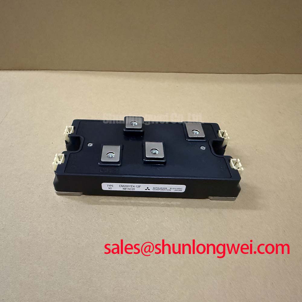
Begin incoming inspection with the module disconnected from every energized circuit: confirm the nameplate identity, inspect the case and terminals, then record cold-state resistance and diode-mode readings against a known-good reference before applying gate drive. The Mitsubishi Electric CM200YE4-12F is an IGBT module with an official rated voltage of 1200 V, an official rated current of 200 A, and a Module package classification. These are the primary catalog specifications supplied for this product; switching frequency, gate limits, short-circuit withstand time, thermal resistance, terminal arrangement, and isolation-test values should be confirmed from the applicable Mitsubishi Electric documentation before commissioning.
For a full-scale converter used in a multi-megawatt onshore or offshore wind turbine, the module should be evaluated inside the complete commutation loop rather than by its voltage and current ratings alone. A long or asymmetrical DC-link bus can add stray inductance, allowing the turn-off current change to create an inductive voltage overshoot. The practical design objective is to minimize the high-current commutation loop and verify the measured collector-emitter peak against the system DC-link boundary during switching tests. The applicable gate resistance, turn-off profile, snubber arrangement, and protection threshold remain system-determined values.
A two-stage soft turn-off strategy is a design consideration for fault handling, not an official CM200YE4-12F specification. The first response can reduce gate drive energy rapidly while avoiding an unnecessarily abrupt current interruption; a subsequent controlled turn-off can then limit the voltage rise detected by the protection circuit. The proposed response time must be checked against the actual driver propagation delay, current sensor bandwidth, fuse behavior, and the module’s documented short-circuit safe operating area. References that describe a response within a particular number of microseconds must not be applied to this module unless the value is confirmed by the relevant manufacturer data.
Type I and Type II short-circuit protection terminology also requires care. The converter designer should define what each protection stage detects, how the gate driver reacts, and whether the sensed signal remains valid during common-mode movement. During commissioning, capture gate-emitter voltage, collector-emitter voltage, phase current, and DC-link voltage on the same time base. A fault waveform that appears to be a device failure may instead involve sensor delay, driver saturation, wiring inductance, or an overvoltage event outside the intended protection sequence.
For a technical reference on Mitsubishi Electric power semiconductor families and high-power modules, consult Mitsubishi Electric Power Semiconductors and High-Power Modules. Its information should be matched to the exact product documentation and production revision used in the equipment.
Field Diagnostics and Commissioning: Suppressing Cres Induced Gate Voltage Spikes
After the static inspection, connect the gate driver only under the approved laboratory isolation procedure and first verify the gate loop polarity. The auxiliary emitter return should be routed as the driver reference, while the main power emitter path should carry the load current through a separate low-impedance route. Mixing these paths can transfer emitter voltage movement into the gate reference and make a valid gate command appear unstable.
High dv/dt across the power terminals can couple through the module’s effective capacitances and raise the off-state gate voltage. A dedicated active Miller clamp is a possible engineering approach where the selected driver supports it, but its suitability depends on the driver’s common-mode range, clamp timing, output impedance, and isolation architecture. A negative gate bias can also be considered for turn-off, including values sometimes used in industrial gate-drive systems, but the permitted gate-emitter range for this exact module must be verified before any negative voltage is applied. The supplied catalog data does not establish a universal negative bias value for CM200YE4-12F.
During a suspected cross-conduction event, inspect both complementary gate signals at the module terminals rather than only at the driver PCB. Compare the off-state gate voltage during the opposite device’s turn-on transition, then examine the common-mode reference and the auxiliary emitter connection. An unexpected pulse may indicate capacitive coupling, ground bounce, probe-loop pickup, or an actual driver timing problem; verify the result with a short-loop differential probe and a known-good signal path before replacing the power module.
High-speed semiconductor fuse coordination should be reviewed with the converter’s prospective fault current, fuse clearing characteristic, cable inductance, and the module’s documented surge limits. I²t coordination is a system calculation and cannot be inferred from the CM200YE4-12F’s 200 A rating alone. The selected fuse must interrupt the fault before damaging energy is transferred to the IGBT, while the protection circuit must avoid nuisance operation during permitted load transients. Any claimed sub-cycle isolation performance requires validation under the actual DC-link and fault topology.
💡 Bench Tip: Use ESD controls and a fully discharged DC link, and record cold-state readings before connecting the gate-driver harness so later changes can be compared with the original baseline.
Transient Dynamics and Electrical Design: Derating and Mismatched Parameters
The 1200 V voltage rating and 200 A current rating are official catalog values, not a complete operating point for a converter. Actual usable current depends on junction temperature, switching loss, case temperature, cooling performance, duty cycle, overload duration, bus voltage, and the manufacturer’s specified safe operating areas. When integrating the module into a wind-turbine full-scale converter, designers should establish thermal and electrical margins from the complete Mitsubishi Electric data set and validate them with measured waveforms under the intended modulation and braking conditions.
Parallel IGBT operation requires both static and dynamic checks. IGBT forward voltage generally has a positive temperature relationship in relevant operating regions, which can support static current sharing, but that observation is a design consideration rather than a guaranteed parallel-sharing specification for this individual module. Differences in gate resistance, driver propagation delay, emitter inductance, thermal contact, and busbar geometry can still create unequal transient current. Each parallel branch should therefore use matched gate-drive paths and symmetrical power interconnects, followed by current-probe measurements during turn-on, turn-off, and overload testing.
Regenerative braking adds another operating condition. A braking chopper may route DC-link energy into a high-power resistor, and the resistor, chopper, fuse, cooling system, and control logic must be evaluated as one energy-absorption chain. The CM200YE4-12F rating does not by itself define the braking resistor value, pulse duration, repetition rate, or allowable energy. Those values are determined from turbine converter dynamics, DC-link control, resistor thermal data, and the module’s switching loss limits.
Where an input rectifier or front-end arrangement is being reviewed, the 2MBI200UR-120-01 may be examined as a related complementary-stage device. This is a neutral topology reference, not a substitute recommendation. Voltage class, current path, gate requirements, isolation, mounting geometry, and protection coordination must be checked independently before pairing any devices in the same converter.
Thyristor trigger circuits used elsewhere in the power cabinet should also be kept electrically distinct from the IGBT gate-drive interface. IGT and VGT are trigger characteristics for a thyristor and must not be transferred to an IGBT gate. If a pulse-train trigger is used for a rectifier or bypass function, the trigger transformer, return reference, pulse amplitude, and pulse duration should be verified from the thyristor’s own documentation. Shared control wiring should be examined for common-mode ground movement and unwanted coupling into the IGBT driver.
CM200YE4-12F Operational Boundaries: Evaluating PCB Gate Loop Layout Symmetry
Inspect the gate-drive board and busbar as a current-return system. The gate signal and its return should follow a compact, consistent path, with the auxiliary emitter reference separated from the high-current emitter conductor. This arrangement reduces mutual coupling and helps prevent the power-current voltage drop from appearing directly in the gate command. The exact trace width, copper thickness, clearance, and creepage requirement must be selected from the working voltage, pollution environment, insulation system, and applicable equipment standard rather than from the module’s 1200 V rating alone.
For the converter’s upper and lower switching positions, keep the gate-loop geometry as similar as the mechanical assembly allows. Avoid routing a gate trace beside a high-current switching node for an extended distance, and avoid creating large probe loops during commissioning. If oscillation is observed, compare the gate waveform at the module pins with the waveform at the driver output, then check the gate resistor position, return path, connector contact condition, and local decoupling. A ringing waveform does not identify one cause without correlation to the collector-emitter waveform and the current transition.
Turn-off overshoot should be addressed at the source by reducing commutation-loop inductance, controlling switching speed through an evaluated gate-drive network, and considering an appropriately validated snubber or clamp. The correct solution is system-dependent. During testing, record the highest collector-emitter voltage, gate-emitter excursion, load current, and DC-link voltage under the most demanding switching condition. If the measured peak approaches the permitted boundary, stop increasing operating stress until the busbar arrangement and protection response have been reviewed.
For engineers comparing power-conversion platforms or reviewing a different device class, the reference article The 1200 V CoolSiC™ MOSFET Advantage in Three provides a separate technology context. It should not be treated as a direct electrical specification for the CM200YE4-12F.
Before release to service, repeat the cold-state pin checks, confirm the gate polarity, inspect insulation distances and mounting interfaces, and compare commissioning waveforms with the approved design record. The CM200YE4-12F should be accepted for a particular wind converter only after its documented ratings, gate-drive limits, thermal path, protection timing, and measured transient behavior have been verified together.