Content last revised on October 31, 2026
Preventing Spurious Faults: Mitigating Commutation Voltage Spikes in 7MBR25SA120-55
I first compare the freewheeling paths with a multimeter in diode mode, keeping the module disconnected from the DC link and the gate terminals under controlled handling. The terminal drawing determines probe polarity; package orientation alone is not a reliable guide. Record readings under the same instrument settings and temperature conditions, then compare corresponding paths. An unusual reading warrants investigation of parallel circuitry, terminal connections, and the measurement setup before attributing it to the semiconductor.
💡 Bench Tip: Use ESD-controlled handling and confirm that the DC link is discharged before probing, then compare cold-state readings with a documented known-good baseline.
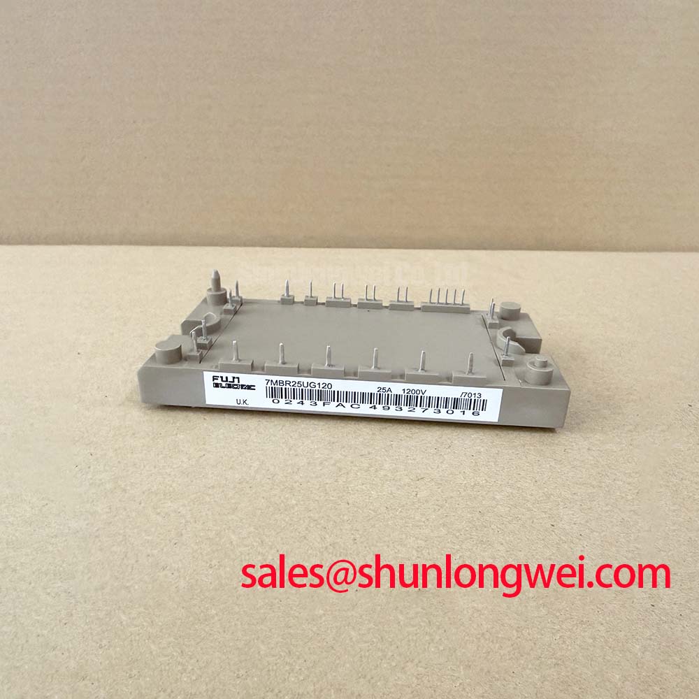
The Fuji Electric 7MBR25SA120-55 has a 1200 V collector-emitter voltage rating and a 25 A DC collector-current rating at 80°C case temperature, both Official Specifications. Its supplied specification also lists 2.10 V collector-emitter saturation voltage; consult the datasheet for the associated test conditions and typical-versus-maximum designation before using this value in a loss calculation. A diode-mode reading is a comparative incoming inspection measurement, not a substitute for those controlled electrical tests.
Design Consideration: static diode measurements cannot establish peak reverse-recovery current or recovery softness. During commutation, a conducting freewheeling diode must recover its blocking capability as current transfers to the opposite switch. The recovery-current peak and the rate at which that current collapses influence ringing, switching stress, and conducted noise. These effects depend on current, junction temperature, switching speed, and the external commutation loop; they should not be assigned a numerical limit from an ordinary multimeter test.
For a repeatable switching investigation, observe collector-emitter voltage and commutation current together using appropriately rated probes. Keep probe connections short and account for measurement-loop pickup before interpreting a narrow voltage spike. Capture the gate waveform at the relevant device reference, rather than only at the driver output. A disturbance seen at the driver board can differ from the voltage actually present across the module’s control terminals.
Engineering Recommendation: minimize the power-loop area to reduce inductive overshoot, while preserving the insulation spacing required by the equipment design. Closely coupled outgoing and return conductors can reduce loop inductance, but this is not permission to narrow clearances between exposed live conductors. Inspect the DC-link connection geometry, local decoupling arrangement, and return-current routing before treating every fault indication as a module defect.
If measurements associate ringing with diode recovery, designers can evaluate turn-on gate-resistance changes or an RC snubber. Slowing turn-on can reduce recovery excitation but increases switching loss; a snubber introduces its own dissipation and voltage stress. Component values should follow the measured waveform, repetitive operating conditions, and thermal capability of the actual assembly. Establish whether the change reduces the disturbance at its source rather than simply altering the fault signal.
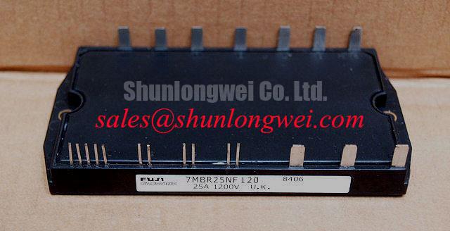
For replacement comparison, 7MBR50UB120 is a separate Fuji Electric reference model, not an automatic substitute. Compare circuit configuration, terminal assignments, mechanical drawing, switching characteristics, and driver requirements before considering interchangeability. A related model designation or a higher current class does not establish compatibility with the existing gate-drive board.
7MBR25SA120-55 Circuit Protection & Reliability: Calibrating Thermal Stress Monitoring
Measure connection resistance with a four-wire micro-ohmmeter only after identifying the actual joint construction and isolating parallel current paths. Place the sense leads across the connection being assessed, not across an arbitrary length of conductor. For bolted connections elsewhere in the module assembly, inspect mating surfaces and fastening condition using the equipment’s assembly instructions. The connection type, fastener size, and tightening torque must follow the applicable mechanical drawing rather than assumptions about the module’s current rating.
Design Consideration: a universal micro-ohm acceptance threshold is inappropriate for every terminal assembly. Contact material, joint area, measurement location, and test temperature affect the result. Use the equipment manufacturer’s acceptance criterion where available, and compare equivalent connections under consistent conditions. Recording the sense-lead positions makes later comparisons more useful than recording an isolated resistance value without a measurement description.
Thermographic inspection can then help locate uneven heating during a controlled load test. Compare corresponding connections at similar current and allow the assembly to approach a stable thermal condition. Reflective metal surfaces can distort apparent temperature, so account for emissivity and viewing angle before interpreting the image. A warm connection may involve contact resistance, unequal current distribution, local cooling, or heat arriving from adjacent conductors; the image alone does not identify the cause.
The 25 A at 80°C case-temperature rating provides a defined electrical reference, not a target for every installation. Design Consideration: evaluate the complete heat path from the module mounting surface through the interface material and heatsink. Check mounting-surface condition, mechanical flatness requirements, and cooling performance against the assembly documentation. Avoid applying press-pack clamping methods, disc-spring preload assumptions, or double-sided cooling procedures to this module without explicit mechanical support.
The supplied Official Specification for short-circuit withstand time is 10 μs. Treat this as a device characteristic under its specified test conditions, not as an allowable intentional protection delay. Engineering Recommendation: assess fault detection, signal filtering, driver propagation, and controlled turn-off as one protection chain. Its response must remain within the applicable device boundary while also controlling the voltage overshoot created when fault current is interrupted.
Dead-time assessment belongs in that same protection review. Compare upper- and lower-switch control timing with the actual gate waveforms, including propagation mismatch and temperature-dependent switching behavior. Complementary gate interlocking can prevent conflicting commands, but it does not eliminate unintended turn-on caused by coupled transients. Keep each gate-current return associated with its own switching reference and examine common return impedance before changing protection thresholds.
Design Consideration: Miller coupling can raise the off-state gate voltage when the opposite switch produces a rapid collector-voltage transition. Gate-return routing, driver sink capability, and any supported clamping function should be evaluated together. Negative gate bias is not a universal correction and should not be assigned a value without the device and driver limits. Likewise, reverse-transfer capacitance is not itself a gate-charge specification; neither an active-clamp setting nor a gate resistor follows directly from a capacitance label.
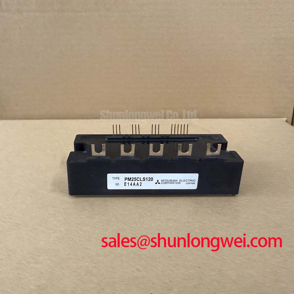
When evaluating integration into a compact industrial inverter or high-speed CNC spindle drive, compare the module against the complete power-stage schematic. Distinguish the incoming rectifier, DC link, inverter switches, and braking circuit before assigning a fault to a particular stage. The 7MBP150RA120-14 is another power-module reference for separate stage-level evaluation; its topology and interfaces must be checked before treating it as a complementary device. Regenerative braking energy, resistor loading, and line-current harmonics remain equipment-level considerations, not characteristics established by the 7MBR25SA120-55 current rating.
7MBR25SA120-55 Operational Boundaries: Evaluating Pollution Degree 3 Creepage Distances Limits
Separate the power circuit from sensitive control electronics before planning any insulation test, and identify the intended test points from the approved procedure. The supplied Official Specification gives 2500 V AC isolation voltage. That rating does not authorize applying the same numerical voltage as a DC insulation-resistance test, nor does it establish an insulation-resistance acceptance threshold. Test voltage, duration, terminal grouping, and acceptance criteria are distinct parts of the procedure.
Design Consideration: an insulation-withstand rating describes performance under stated test conditions; it is not a continuous working-voltage declaration or proof of complete equipment safety compliance. A bench insulation measurement also cannot certify the condition of an internal ceramic layer. It can reveal an abnormal electrical path under the selected test conditions, but determining its origin requires the approved diagnostic process and assessment of the surrounding assembly.
Inspect accessible insulating surfaces for conductive dust, moisture, residue, and damage before energizing the equipment. Pay attention to terminal exits, mounting interfaces, and nearby conductors where contamination can create an external leakage path. Cleaning should follow the assembly’s material-compatible process, with adequate drying before retesting. Record the condition before and after cleaning so a changed reading is not automatically attributed to an internal device fault.
For a Pollution Degree 3 assessment, select the applicable equipment standard and evaluate working voltage, insulation function, material group, and the actual enclosure environment. Creepage follows the insulating surface; clearance is the shortest air path. These distances require separate assessment. Neither the 1200 V semiconductor blocking rating nor the 2500 V AC isolation specification supplies a universal spacing requirement for the surrounding board and buswork.
Engineering Recommendation: preserve the approved insulation geometry when replacing a module, especially where nearby busbars, fastening hardware, or cable terminations can change the shortest path. Check for trapped debris and displaced insulating parts after assembly. Any revised conductor arrangement should be reviewed against the equipment’s insulation-coordination requirements rather than accepted because it clears the package mechanically.
For manufacturer context, Fuji Electric Power Semiconductor & IPM Modules provides the relevant product-family reference. The separate Wide Bandgap Revolution technical article discusses broader switching and integration considerations; it does not establish specifications or insulation-test limits for this model. Close the inspection record with the terminal map used, instrument identification, test conditions, connection-resistance observations, and the approved insulation-test result so the next engineer can reproduce the assessment.