At the very heart of modern power electronics—from the drivetrain of an electric vehicle to the inverters in a solar farm—lies a remarkable semiconductor device: the Insulated Gate Bipolar Transistor (IGBT). The IGBT acts as a high-speed, high-power switch, but its true elegance lies in how it operates.
To master its application, one must first understand its core working principle: a sophisticated, unidirectional switching mechanism governed entirely by voltage.
This comprehensive guide will demystify the IGBT’s operation, breaking down its turn-on and turn-off processes, exploring its inherent characteristics, and addressing the potential risks every engineer must consider.
The Foundation: The Simplicity and Power of Voltage Control
The most defining characteristic of an IGBT is that it is a voltage-controlled device. This marks a fundamental distinction from its predecessor, the BJT (Bipolar Junction Transistor), which is current-controlled.
To control an IGBT, you simply apply a voltage signal to its Gate terminal.
- To Turn On: Apply a positive voltage (VGE) between the Gate and the Emitter that exceeds the device’s threshold voltage (Vth).
- To Turn Off: Remove the gate voltage (set VGE to 0V) or apply a small negative voltage.
This MOSFET-like input behavior provides two enormous engineering advantages:
- Simplified Drive Circuitry: A voltage-controlled gate requires virtually zero current to maintain its state (either on or off), drastically simplifying the design of the gate driver circuit and reducing overall power consumption.
- Seamless Digital Integration: Voltage signals are easily generated and controlled by microcontrollers (MCUs) and other digital logic, allowing for precise, high-speed control in complex systems.
This principle of voltage control is the cornerstone that makes the IGBT both powerful and accessible.
The Art of Turning On: From Channel Inversion to Conductivity Modulation
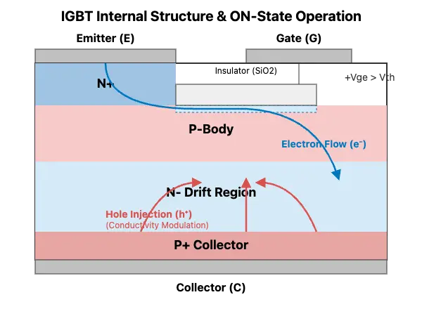
When the conditions for conduction are met (VGE > Vth and a positive voltage on the Collector relative to the Emitter), a brilliant two-stage process unfolds within the IGBT’s silicon structure.
1. Gate Activation & Channel Formation:
The initial action is purely that of a MOSFET. The positive gate voltage attracts electrons in the p-body region beneath the gate, forming a thin n-type inversion layer. This layer acts as a conductive bridge, or channel, allowing electrons to begin flowing from the Emitter into the N-drift region. This “opens the door” for current flow.
2. Performance Amplification: Conductivity Modulation
Once the electron channel is formed, the IGBT’s true advantage comes into play. As electrons flow into the wide, high-resistivity N-drift region, they attract minority carriers (holes) from the P+ Collector region. The N-drift region is subsequently flooded with a high concentration of both electrons and holes.
This phenomenon is known as Conductivity Modulation. It dramatically reduces the electrical resistance of the N-drift region, which is the component designed to block high voltages.
Conductivity modulation is the key to resolving a classic power semiconductor trade-off. It allows the IGBT to simultaneously feature:
- High Blocking Voltage: Thanks to the thick, lightly doped N-drift region.
- Low Conduction Loss: Thanks to the drastically reduced on-state resistance (resulting in a low Vce(sat)).
This dual capability is precisely why IGBTs excel over traditional Power MOSFETs in high-voltage, high-current applications.
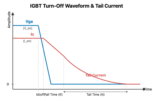
The Challenge of Turning Off: The Inevitable Tail Current
When the gate voltage is removed, the MOSFET channel vanishes almost instantly, cutting off the primary path for electrons. However, the process is not yet complete.
Because the IGBT is a minority carrier device, the N-drift region is still saturated with charge carriers (holes) left over from the conductivity modulation process. These carriers must be swept out or recombine before the device can fully block current. This lingering flow of current during the turn-off phase is known as Tail Current.
This inherent tail current has two significant consequences:
- Increased Switching Losses: During the tail current period, the voltage across the device is already rising to the full blocking voltage. The simultaneous presence of current and voltage (P = V * I) creates significant energy loss, which manifests as heat.
- Limited Switching Frequency: The tail current extends the total time required for the IGBT to turn off completely. This turn-off time (tf) is a primary factor limiting the maximum operating frequency of the device, which is why IGBTs are generally slower than MOSFETs.
Defining the Boundaries: Key Characteristics & Design Considerations
Understanding the following characteristics is crucial for successful and reliable system design.
1. Transfer Characteristics: A Linear Control Blueprint
The IGBT’s transfer characteristic curve (Collector Current, Ic vs. Gate-Emitter Voltage, VGE) closely resembles that of a Power MOSFET. Below the threshold voltage (Vth), the device is off. Above the threshold, the collector current increases in a reasonably linear fashion with the gate voltage. This predictable, linear relationship allows engineers to precisely modulate the current flow by adjusting the gate voltage, a vital feature for applications like motor control.
2. Unidirectional Switch: A Critical Design Constraint
An IGBT is fundamentally a unidirectional device. It is designed to switch current flowing in only one direction: from the Collector to the Emitter. It cannot block significant reverse voltage or control reverse current flow.
Practical Implication: In applications that involve inductive loads or AC waveforms (like inverters and motor drives), it is mandatory to place a Freewheeling Diode in anti-parallel with the IGBT. This diode provides a safe path for the reverse current when the IGBT turns off, protecting it from destructive reverse voltage transients.
3. The Hidden Danger: Latch-Up and Its Prevention
Deep within the IGBT’s silicon layers lies a parasitic structure equivalent to a thyristor (formed by the internal NPN and PNP transistors). Under extreme conditions—such as a massive current surge far exceeding the device’s rating or excessive temperature—this parasitic thyristor can trigger and turn on. This is known as Latch-Up.
Once latched, the gate loses all control over the device. The IGBT becomes stuck in the “on” state, conducting a large current that can only be stopped by forcibly interrupting the external circuit. If not addressed immediately, latch-up leads to thermal runaway and catastrophic device failure.
Modern IGBTs are engineered with advanced cell designs to be highly resistant to latch-up. However, designers must still ensure the device always operates within its specified Safe Operating Area (SOA). Implementing robust over-current and short-circuit protection in the gate driver is a non-negotiable aspect of reliable system design.
Conclusion: The Art of the Engineering Trade-Off
The IGBT’s working principle is a brilliant story of engineering trade-offs, embodying a “simple on the outside, complex on the inside” duality.
- Externally, it offers the elegant simplicity of voltage control, empowering engineers to manage immense power with finesse.
- Internally, its reliance on a complex minority carrier mechanism grants it the gift of conductivity modulation (low conduction loss at high voltage) but also imposes the limitation of tail current (slower switching speed) and the risk of latch-up.
For the power electronics engineer, a deep understanding of these intertwined characteristics is the foundation for intelligent device selection, efficient circuit design, and robust system protection. Mastering the art of the IGBT is mastering the art of modern power conversion itself.