


Content last revised on September 30, 2026
Field Diagnostics & Commissioning: Dynamic Power Loss Dissipation and Multi-R in FP40R12KT3 Topologies
| Manufacturer | Infineon |
| Part Number | FP40R12KT3 |
| Product Category | IGBT Module with inverter, rectifier, brake chopper, and internal NTC functions |
| Inverter IGBT VCES | 1200 V |
| IGBT Rth(j-c) | 0.60 K/W |
| Rectifier VRRM | 1600 V |
| Brake Chopper IC | 40 A |
| Integrated NTC R25 | 5.0 kΩ |
Probe the DC link, brake chopper path, gate signals, and NTC resistance before energizing a repaired commercial string inverter or micro-grid energy storage converter. The initial objective is to separate a switching-device problem from excessive bus inductance, incorrect braking-resistor loading, inadequate heat transfer, or a temperature-sensing fault.
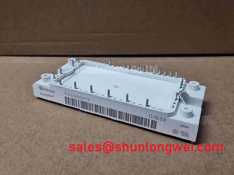
The FP40R12KT3 combines an inverter IGBT section, a rectifier section, a brake chopper section, and an integrated thermistor. Its official inverter collector-emitter voltage rating is VCES = 1200 V. The brake chopper section has an official maximum collector-current rating of IC = 40 A, while the rectifier stage is specified at VRRM = 1600 V. These figures define device-level electrical boundaries; they do not by themselves establish the allowable inverter bus voltage, switching frequency, braking duty cycle, or heat-sink performance of a complete system.
For a field assessment, record the actual DC-link voltage during charging, regeneration, and braking events. Then compare the measured switching waveform with the known-good phase leg or a reference unit. A high collector-emitter overshoot during turn-off may point to commutation-loop inductance, unbalanced busbar geometry, gate-loop coupling, or an unsuitable switching transition. The correct response is waveform verification rather than assigning the fault to the module from a single voltage reading.
The official junction-to-case thermal resistance for the IGBT section is Rth(j-c) = 0.60 K/W. Use this value with the system heat-sink and interface conditions to construct the thermal path used by the design team. A transient thermal model may include multiple RC branches when the brake resistor is repeatedly absorbing regenerative energy, but the time constants and thermal impedances must come from the applicable manufacturer documentation or validated laboratory measurements. They should not be inferred from the steady-state figure alone.
In a solar inverter, the brake chopper can be exposed to short energy pulses that are not represented by the average converter load. Capture the brake command, DC-link rise, chopper collector-emitter waveform, and heat-sink temperature together. If the chopper turns on correctly but the bus continues to rise, inspect the braking resistor, its cabling, fuse path, control isolation, and resistor thermal condition before replacing the module. If the switching edge contains ringing, inspect the positive and return busbar paths as a complete commutation loop.
For mechanical installation, use a calibrated torque screwdriver and tighten the module in a cross pattern. The specified pre-fixation range is 0.5 to 0.7 N·m, followed by a final range of 1.1 to 1.5 N·m. The stated mechanical objective is even interface seating, controlled grease spreading, and metal-to-metal contact pressure without baseplate distortion. PCB terminal soldering is specified at 260 °C ± 5 °C for no more than 10 seconds, using a controlled soldering iron or wave profile to avoid mechanical shear on the internal terminal pins.
Where a repair requires evaluation of a related high-power module, engineers may review BSM100GB120DLC as a separate compatible-device candidate. Any substitution still requires confirmation of electrical topology, terminal arrangement, thermal interface, drive requirements, and protection coordination in the original equipment.
Preventing Spurious Faults: Mitigating Hard Switching Transients via A Guidelines for FP40R12KT3
Measure the gate-emitter waveform and collector-emitter voltage at the same switching event when a repaired inverter reports an intermittent overcurrent or desaturation fault. Use a properly rated differential probe and a short, low-inductance measurement connection so that probe wiring does not create a false ringing signature.
The 1200 V VCES rating is an official voltage specification, not a target for repetitive switching overshoot. During turn-off, the stray inductance of the DC-link and commutation path can produce a voltage excursion that depends on current, transition speed, layout, and the connected diode path. Minimize the high-current loop area and keep the upper and return busbar paths geometrically paired. The final peak voltage margin must be confirmed by oscilloscope testing at the intended operating current and temperature.
A two-stage soft turn-off strategy can be considered when the gate driver and protection controller support it. The protection sequence, fault detection delay, gate-current control, and safe turn-off behavior must be established by the system design rather than attributed to the module itself. The supplied official data does not establish a model-specific short-circuit response time or a guaranteed short-circuit safe-operating interval, so an assumed value such as a sub-10-microsecond limit should not be used as a design guarantee.
Check the gate loop for shared impedance between the driver return and power-current paths. A gate waveform that changes when the brake chopper operates may indicate common-source or common-return coupling, probe reference error, Miller injection, or control-ground movement. Designers should keep the gate-drive path compact, maintain a clear return path, and verify turn-on and turn-off behavior under the highest intended commutation stress.
Switching-frequency evaluation should be based on measured semiconductor loss and thermal response rather than a generic frequency label. At each intended operating point, record phase current, duty cycle, bus voltage, switching temperature, heat-sink temperature, and fault history. The result should be compared with the available thermal design margin and the module’s official thermal resistance. Cooling airflow, filter loading, enclosure temperature, and heat-sink contact condition remain system-level variables.
For the rectifier portion, the official repetitive peak reverse voltage is VRRM = 1600 V. Verify that commutation transients and line-side disturbances remain within the applicable rectifier design boundary. The rectifier and inverter should be assessed as one power-conversion topology because an abnormal front-end waveform can influence DC-link ripple, braking activity, and inverter switching stress.
For related front-end topology studies, the surrounding power path may also be reviewed with the separate BSM75GP120 device page. This is a neutral topology reference, not a claim that the two products are interchangeable or electrically equivalent.
🔧 Bench Diagnostic: Disconnect the DC bus and allow the documented discharge circuit to complete before removing gate, power, or thermistor connections.
Benchtop Waveform Tuning: Mitigating Stress via DC-Bus Operating Voltage Headroom Derating on FP40R12KT3
Capture the DC-bus waveform at the module terminals during acceleration, regeneration, and brake-chopper activation, then compare the measured peak with the converter’s specified operating boundary and the module’s 1200 V VCES rating. This test should include the actual busbar, capacitor bank, braking resistor, and gate-driver configuration used in the equipment.
Voltage headroom is influenced by more than the nominal DC-link setting. Busbar parasitic inductance, capacitor placement, commutation current, gate resistance, diode recovery, and control timing can combine to raise the instantaneous collector-emitter voltage. The engineering objective is to suppress overshoot by reducing the high-current loop inductance and controlling switching transitions, followed by verification with a high-bandwidth differential measurement.
Altitude and terrestrial neutron exposure require source-based reliability analysis. The supplied product data does not provide a cosmic-ray or neutron-induced Single Event Burnout model, an altitude derating curve, a FIT rate, or an SEB voltage threshold for this specific module. Do not calculate a field failure rate from the 1200 V rating alone. If the converter is intended for operation above the altitude used in its original qualification, the system owner should obtain the applicable manufacturer reliability data and conduct the required environmental assessment.
Benchtop tuning should begin with a controlled low-energy switching condition and progress only after the waveform, gate signal, and protection response are stable. The test engineer should inspect both the positive and negative bus paths, capacitor terminal connections, laminated busbar interfaces, and brake-resistor conductors. A mechanically loose connection can create waveform behavior that resembles a semiconductor fault.
The brake chopper rating provides an important boundary for regenerative-energy analysis. The official maximum collector-current rating is 40 A, but the permissible pulse duration, repetition pattern, junction temperature, and external resistor energy must be coordinated with the complete thermal design. Confirm the resistor’s pulse capability separately and monitor the NTC signal during repeated braking events.
The integrated sensor is specified at R25 = 5.0 kΩ. Measure the thermistor with the module isolated from the control circuit, then compare the result against the equipment’s sensor interpretation and temperature table. A control system that applies the wrong NTC curve can generate misleading thermal alarms or suppress protection without proving that the semiconductor temperature is acceptable.
For broader multi-level inverter and energy-storage topology considerations, the engineering team can consult Peak Efficiency in Solar and Energy Storage. The article should be used as a topology reference; it does not replace the FP40R12KT3 electrical and thermal verification required for a specific converter.
FP40R12KT3 Operational Boundaries: Evaluating Thermal Feedback Limits
Measure the NTC resistance at a known stabilized temperature and compare the controller’s reported temperature with an independent thermal measurement at the module case. This quickly separates sensor interpretation, interface contact, and cooling-path questions before dynamic current-sharing tests begin.
The integrated NTC has an official resistance value of 5.0 kΩ at 25 °C. This is a sensor specification, not a direct junction-temperature measurement. The control system should use the correct resistance-temperature relationship for the installed component and validate the complete sensing chain, including connector resistance, analog filtering, scaling, isolation, and alarm thresholds.
Static current sharing in parallel semiconductor paths can benefit from the positive temperature coefficient commonly associated with IGBT saturation voltage, but the exact behavior must be verified for the selected operating point and device arrangement. Dynamic sharing is more sensitive to gate-loop impedance, driver propagation mismatch, emitter-return geometry, and commutation inductance. Match the physical gate-loop routing and return paths as closely as practical, then confirm current balance with synchronized voltage and current measurements.
Thermal evaluation should include the module mounting interface. Apply the specified cross-pattern sequence, beginning at 0.5 to 0.7 N·m and completing the final tightening at 1.1 to 1.5 N·m. The heat-transfer result depends on the interface material, surface condition, heat-sink flatness, mounting pattern, and enclosure airflow. A correct torque value cannot compensate for a damaged mounting surface or uneven interface layer.
The official IGBT thermal resistance of 0.60 K/W should be combined with measured case temperature and calculated semiconductor loss when checking thermal feedback limits. Loss estimation should include conduction and switching components at the actual current, voltage, gate-drive condition, and modulation pattern. If the calculated result conflicts with the temperature sensor, repeat the measurement using an independent instrument and inspect the sensor wiring before changing protection thresholds.
Infineon’s public information on IGBT discretes and co-pack diodes provides useful background for comparing device families, while its automotive-qualified power modules page belongs to a different qualification context. Neither reference changes the official ratings or validation requirements for the FP40R12KT3.
When integrating this module into a commercial string inverter or micro-grid energy-storage system, designers should verify the complete protection chain under normal switching, regenerative braking, cooling degradation, and control restart conditions. The final decision should be based on measured electrical peaks, thermal response, sensor agreement, and the equipment’s documented operating limits.