Content last revised on March 22, 2026
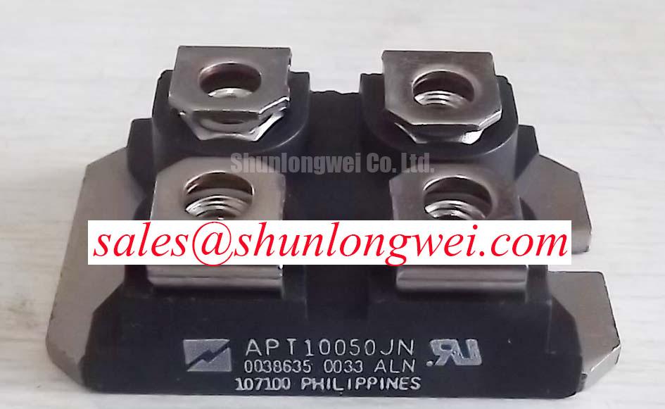
APT10050JN Microsemi 1000V 21A N-Channel Power MOSFET
The APT10050JN is a high-performance N-channel Power MOSFET utilizing Advanced Power Technology (now Microsemi) proprietary Power MOS V technology. This device is specifically engineered to deliver low on-resistance and high switching speed in a compact, isolated SOT-227 (ISOTOP) package. By providing a high 1000V drain-source breakdown voltage, it addresses the stringent requirements of high-frequency power conversion and high-voltage industrial applications where thermal efficiency and electrical isolation are paramount.
UVP Statement: Achieving superior high-frequency switching efficiency and thermal reliability through an isolated 1000V power stage in a compact SOT-227 footprint.
- Top Specs: 1000V | 21A | 0.50 Ohms RDS(on)
- Key Benefits: Reduces cooling complexity with 2500V RMS isolation; optimizes power density in high-frequency SMPS.
One of the primary concerns for engineers evaluating the APT10050JN is how the isolated package impacts thermal design. Because the SOT-227 package features an internal alumina substrate, the device offers 2500V isolation between the terminals and the mounting base, allowing multiple modules to be mounted on a single common heatsink without additional insulating pads. For high-frequency SMPS designs requiring a 1000V rating and isolated thermal management, the APT10050JN is the optimal choice.
Application Scenarios & Value
Achieving System-Level Efficiency in High-Frequency Power Conversion
Engineers often face the challenge of managing high-voltage transients while maintaining switching speed in Power Factor Correction (PFC stage) and Switch Mode Power Supplies (SMPS). In a typical UPS (Uninterruptible Power Supply) design, the APT10050JN serves as a critical switching element. The low gate charge (Qg) of this MOSFET allows for faster transition times, which directly translates to lower switching losses—a vital factor when operating at frequencies above 100 kHz.
Consider the design of a high-voltage industrial plasma generator. The APT10050JN must handle the reactive power and rapid load changes inherent in plasma ignition. With a maximum continuous drain current (ID) of 21A and a rugged avalanche energy rating, this MOSFET provides the necessary margin to survive voltage spikes and inductive kickbacks. For systems requiring even higher current handling, the related IXFN180N10 offers a different performance profile for low-voltage, high-current applications.
This MOSFET is also widely utilized in welding power supplies and high-frequency induction heating. By naturalizing the SOT-227 package into these designs, manufacturers can achieve a higher power-to-weight ratio compared to traditional discrete TO-247 solutions. The integration of APT10050JN into industrial inverters compliant with IEC 61800-3 standards ensures that the switching characteristics are stable across wide temperature ranges, supporting long-term system reliability.
Industry Insights & Strategic Advantage
Strategic Reliability in the Evolution of Industrial Power Density
The global trend toward "Green Energy" and higher efficiency standards is driving a shift toward high-voltage architectures. The APT10050JN aligns with this strategic transition by offering a 1000V rating that accommodates the higher DC bus voltages increasingly common in renewable energy storage and EV inverter testing equipment. This move toward higher voltages reduces current levels for the same power output, thereby decreasing ohmic losses in cabling and interconnects.
A technical deep dive into the RDS(on) of 0.50 Ohms reveals how Microsemi has optimized the silicon structure. To visualize this, think of RDS(on) as the diameter of a water pipe: the lower the resistance (the wider the pipe), the less energy is wasted as heat during conduction. In high-power systems, even fractional reductions in resistance can lead to significant energy savings over the lifecycle of the equipment. Furthermore, the Power MOS V process ensures low parasitic capacitances, which is the "electronic friction" that slows down switching transitions. Minimizing this friction allows for cleaner waveforms and reduced Electromagnetic Interference (EMI) filtering requirements.
For more detailed insights on how power semiconductors are evolving to meet these challenges, you can explore our analysis on IGBT and Power MOSFET Technologies. Understanding these dynamics is essential for balancing Thermal Management and Switching Efficiency in next-generation designs.
Key Parameter Overview
Decoding technical specifications for high-voltage stability
The following table summarizes the critical electrical and thermal characteristics of the APT10050JN, as specified in the manufacturer's technical documentation.
| Parameter | Specification Value | Engineering Significance |
|---|---|---|
| Drain-Source Voltage (VDSS) | 1000V | Provides safety margin for 600V-800V DC bus applications. |
| Continuous Drain Current (ID) | 21A (at TC = 25°C) | Defined current limit for conduction loss calculations. |
| On-Resistance (RDS(on)) | 0.50 Ohms (Max) | Determines the static power dissipation during the "ON" state. |
| Package Type | SOT-227 (ISOTOP) | Isolated mounting simplifies thermal assembly and increases density. |
| Isolation Voltage | 2500V RMS | Ensures safety and compliance in high-voltage industrial equipment. |
| Total Gate Charge (Qg) | 190nC (Typical) | Key metric for selecting appropriate gate driver current capacity. |
Download the APT10050JN datasheet for detailed specifications and performance curves.
Technical FAQ
How does the 2500V isolation in the SOT-227 package benefit multi-device systems?
The internal isolation allows the APT10050JN to be mounted directly to a metal heatsink without an external mica or silicone pad. This reduces the thermal interface layers, lowering the total junction-to-ambient thermal resistance and allowing multiple modules to share one cooling structure without electrical shorting.
What is the engineering impact of the 1000V VDSS rating in PFC applications?
In PFC stage designs, the MOSFET is often subjected to high-voltage transients during startup or load shedding. A 1000V rating provides a robust buffer over the standard 400V-500V DC bus, significantly reducing the risk of avalanche breakdown and improving long-term reliability in unstable grid conditions.
How should the Gate Charge (Qg) of 190nC influence gate driver selection?
The gate charge determines the amount of current the Gate Drive circuit must supply to switch the MOSFET at a specific speed. With 190nC, the driver must be capable of providing sufficient peak current to ensure fast transitions, thereby minimizing switching losses and preventing linear-mode operation which could lead to thermal failure.
Does the APT10050JN require a snubber circuit in high-frequency SMPS?
While the Power MOS V technology is inherently rugged, high-frequency switching involving parasitic inductance in the PCB layout can cause ringing. A Snubber Circuit is often recommended to damp these oscillations, especially when the VDSS approaches its 1000V limit, to ensure operation remains within the Safe Operating Area (SOA).
What is the primary benefit of the low RDS(on) of 0.50 Ohms in industrial heating?
Low RDS(on) minimizes conduction losses, which is critical in high-duty cycle applications like induction heating. By reducing the heat generated at the silicon level, it allows for smaller heatsinks and enhances the overall energy efficiency of the industrial converter system.
For procurement professionals and design engineers, the APT10050JN represents a proven solution for high-voltage power management. Its combination of 1000V capability and the thermally efficient SOT-227 package makes it a versatile component for demanding industrial environments. For further technical comparison, please refer to our Power Semiconductor Selection Guide.