



Content last revised on September 29, 2026
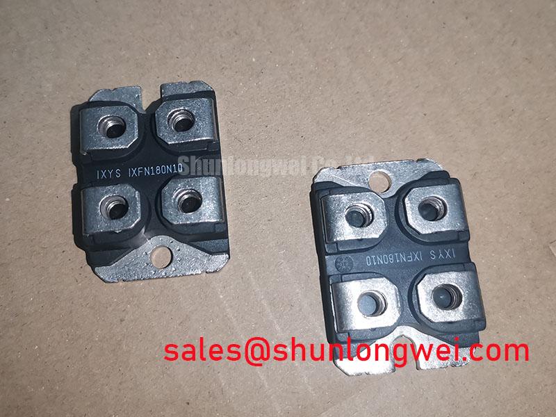
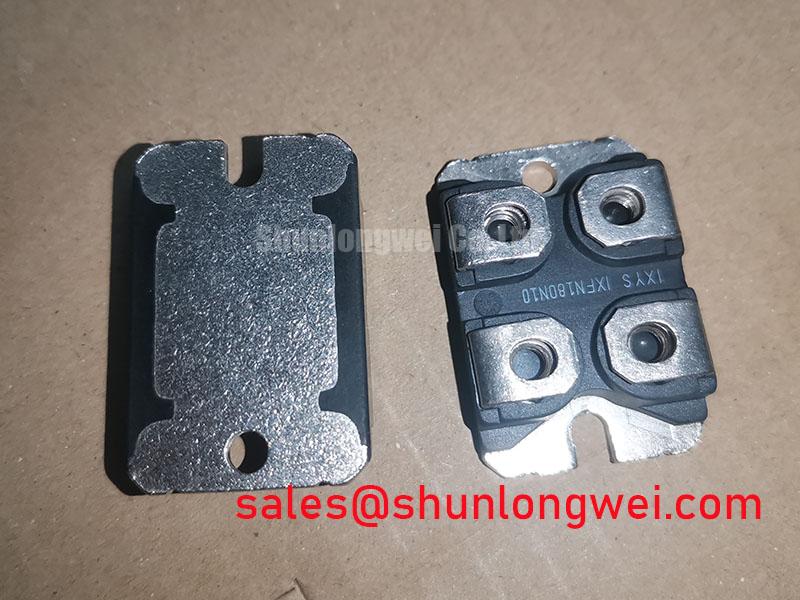
IXFN180N10 Circuit Protection and Reliability for Braking Resistors and Chopper Transistors
| Hardware Specification | Value |
|---|---|
| Manufacturer | IXYS |
| Model | IXFN180N10 |
| Product Category | Power MOSFET Module |
| Drain-Source Voltage Rating | 100 V |
| Rated Drain Current | 180 A under specified datasheet conditions |
| Package | Module |
Measure the chopper path with the DC link isolated, then compare the gate control signal, power terminals, and braking resistor connection with the known-good circuit before energizing the inverter. The IXFN180N10 is an IXYS power MOSFET module with a 100 V drain-source voltage rating and a 180 A rated drain current under specified datasheet conditions. These values define the component-level reference point; the actual braking circuit remains dependent on the DC-link voltage, pulse duration, load inertia, switching frequency, resistor network, protection threshold, and thermal path established by the equipment designer.
In a compact industrial inverter or high-speed CNC spindle drive, the braking branch must be checked as a complete energy path rather than as an isolated semiconductor replacement. During deceleration, the motor can return energy to the DC link. The braking resistor and chopper transistor must work together so that the link voltage remains within the limits established by the system design. Confirm the resistor wiring, contact integrity, pulse rating, and cooling condition while the equipment is disconnected. A resistance measurement alone does not prove that the resistor can absorb the required repetitive braking energy.
Use an oscilloscope with suitable differential and current probes to observe the DC-link rise, chopper gate command, drain-source voltage behavior, and braking current during a controlled bench test. A missing gate transition, an unusually slow edge, or ringing that appears only during load operation may indicate a driver, layout, snubber, or parasitic inductance issue rather than a failed power module alone. The measurement should be compared with the original signal path and the equipment protection thresholds.
Protection coordination also includes the semiconductor fuse or upstream protective device. The fuse selection must be evaluated against the pulse current profile and the applicable I²t relationship, while the chopper device must be assessed against its applicable safe operating area and transient limits. Do not infer short-circuit endurance from the rated drain current. A device that survives a static resistance check can still be damaged by a fast overvoltage event, an incorrectly timed gate command, or a braking resistor that has changed value under heat.
Keep the high-current braking loop physically compact and route the gate return separately from the power return where the drive architecture permits. The objective is to reduce common impedance and suppress unwanted gate movement during rapid voltage transitions. Clearance and creepage must be determined from the working voltage, pollution environment, insulation system, and applicable equipment standard. The module package alone does not establish the finished assembly insulation distance.
IXFN180N10 Thermal and Electrical Optimization for Hard Switching Transients
Capture the gate signal and power-terminal waveform at the module terminals when a hard-switching fault is suspected, because a probe placed far from the device can hide the voltage overshoot that stresses the silicon. The first comparison should include gate amplitude, turn-on and turn-off timing, Miller-region behavior, and the relationship between the command signal and the power transition. These observations help separate a driver problem from a thermal or commutation problem.
A short-circuit protection design should detect abnormal conduction rapidly and remove gate drive in a controlled manner. The actual sensing method, current feedback path, blanking behavior, and protection response must be verified from the equipment schematic. A nominal response target such as less than ten microseconds should not be treated as an IXFN180N10 factory specification unless it is explicitly documented for the exact device and drive circuit.
Controlled turn-off is a design consideration for limiting the voltage excursion caused by stored energy in the commutation loop. A two-stage response may use a rapid initial reduction followed by a controlled final gate discharge, but the timing and gate impedance must be established through switching tests. The correct setting depends on DC-link voltage, stray inductance, load current, driver capability, and the device’s applicable safe operating area. Verify the peak device voltage against the actual DC-link conditions rather than relying on a nominal waveform captured at a remote test point.
Thermal evaluation should use the transient thermal impedance information available for the exact semiconductor construction and operating condition. The junction temperature during a braking pulse depends on the starting case temperature, pulse width, duty cycle, mounting interface, heatsink response, and the complete Zth network. A single steady-state heatsink calculation cannot represent a short repetitive pulse. Record case temperature and switching repetition during the test so that the pulse peak and the average thermal load are evaluated together.
When installing the module on a prepared heatsink, apply the thermal interface material evenly and avoid areas where excess compound can migrate toward terminals. A controlled interface thickness in the approximate 50 to 80 micrometre range is a general engineering starting point for suitable materials, not an IXFN180N10 factory specification. The final interface depends on the compound, surface flatness, baseplate condition, clamping method, and supplier instructions. Inspect the contact pattern after a controlled trial assembly when the thermal path is critical.
Common-mode transient immunity is a system property of the isolation barrier, gate driver, PCB geometry, and return path. In industrial drive boards, an optocoupler or digital isolator must be evaluated for its specified CMTI under the actual common-mode transition, while the power loop and control loop should be kept from sharing unnecessary impedance. The presence of an isolated driver does not by itself prove immunity to every switching transient. Check the isolated supply, driver output reference, gate return, and fault feedback path with differential measurements.
Assembly Integrity and Layout Architecture for Thermal Paste and Mechanical Control
Inspect the heatsink contact imprint, fastener seating, terminal condition, and baseplate alignment when a module shows abnormal case temperature or intermittent switching behavior. Uneven contact pressure can create local thermal resistance, while excessive compound can reduce mechanical stability and contaminate nearby insulation surfaces. The module package designation does not specify a universal screw size, torque value, baseplate flatness, or heatsink interface procedure.
Prepare the mating surfaces by removing old interface material without scoring the mounting area, then check for burrs, contamination, and visible curvature. The baseplate and heatsink should be evaluated as a pair. If the assembly uses multiple screws, tighten them progressively in a cross-pattern so that the pressure develops evenly across the device. The exact torque sequence, torque value, washer arrangement, and thread treatment should follow the mechanical documentation for the equipment and the fastener manufacturer.
Thermal paste thickness must be controlled by the interface materials and surface condition. An approximate 50 to 100 micrometre target is a general design consideration for a thin, continuous film, not a guaranteed requirement for this specific IXYS module. Voids, dry regions, trapped debris, and excessive compound can all increase the effective thermal path. Where the application is sensitive to thermal cycling, document the material batch, application method, curing or settling requirements, and post-assembly inspection result.
Electrical layout should keep the high di/dt power loop short and separate from the gate-drive loop. The gate resistor, return conductor, isolation barrier, current sensor, and fault feedback routing should be placed according to the switching topology and measured waveform. Avoid treating a long PCB trace or mounting strap as an electrically neutral connection. Its inductance can alter the gate voltage seen at the module and can increase turn-off overshoot during braking or short-circuit interruption.
Parallel semiconductor operation requires separate verification of static and dynamic current sharing. A positive temperature coefficient can assist static sharing in some operating regions, but it does not eliminate differences caused by gate-loop inductance, threshold variation, driver timing, stray inductance, or thermal coupling. If multiple devices are used in a system, designers should measure current sharing during the actual switching transition and under the intended thermal gradient. The IXFN180N10 rating does not establish a parallel-operation guarantee.
Terminal maintenance should include a visual check for discoloration, looseness, cracked insulation, and evidence of repeated thermal cycling. Measure contact resistance only with a method appropriate to the connection and interpret the result alongside temperature-rise observations. A clean static measurement does not replace a loaded thermal inspection.
Maintenance Note: Monitor contact temperature during scheduled operation and keep the heatsink airflow path clear before thermal drift develops into a switching fault.
For broader application work involving gate-drive isolation, thermal interfaces, commutation loops, and protection coordination, consult the IGBT Design and Integration reference as a system-level engineering resource. It should complement, not replace, the device-specific mechanical and electrical documentation used for the repair.
Transient Dynamics and High-Altitude Cosmic-Ray Considerations for IXFN180N10
Record the failed device location, DC-link voltage, switching state, ambient conditions, and the surrounding protection waveform before attributing a catastrophic short to cosmic-ray or altitude effects. A failed power module can result from excessive voltage, gate-drive malfunction, poor thermal contact, commutation overshoot, contamination, or an upstream protection mismatch. The first diagnostic step is to preserve the evidence and compare the damaged position with the known-good phase or braking branch.
Single-event burnout is a specialized reliability topic that requires a device-specific failure model, semiconductor structure information, operating voltage distribution, particle environment, and validated test data. Terrestrial neutron flux can vary with altitude and installation environment, but no field failure rate, FIT value, safe altitude limit, or SEB probability should be assigned to IXFN180N10 without an authoritative source covering the exact device and operating condition.
DC-bus headroom should be treated as a system design variable. The engineer should identify the highest repetitive voltage, the maximum switching overshoot, the duration of the excursion, and the protection response under the worst credible load condition. The 100 V drain-source rating is a component parameter, but it does not establish a permitted operating voltage for every converter topology, nor does it define an altitude derating curve or transient immunity limit.
Use controlled testing with appropriately rated probes, barriers, discharge procedures, and test fixtures. Compare the measured voltage at the module terminals with the voltage at the DC link and review the difference caused by the commutation path. If the terminal waveform contains narrow spikes, investigate loop inductance, snubber condition, diode recovery behavior, gate timing, and measurement technique before assigning the event to a radiation mechanism.
Galvanic isolation also matters when a DC link is connected to an industrial control board. The principles described in galvanic isolation provide useful context for separating functional signal paths from power domains. The finished equipment still requires verification of insulation coordination, creepage, clearance, dielectric testing, and enclosure conditions under the applicable product standard.
For compact inverter and CNC spindle applications, the equipment designer should correlate any suspected high-altitude event with the actual operating voltage, switching duty, cooling performance, and maintenance history.
When the module is returned for evaluation, retain the driver board, gate resistor, fuse, braking resistor, heatsink interface, and any snubber components with the device. These surrounding parts can reveal whether the event began as an electrical overstress, a thermal-interface problem, a protection-timing issue, or a mechanical connection failure. The available evidence should guide further laboratory analysis rather than an unsupported FIT or SEB conclusion.