
Content last revised on September 21, 2026
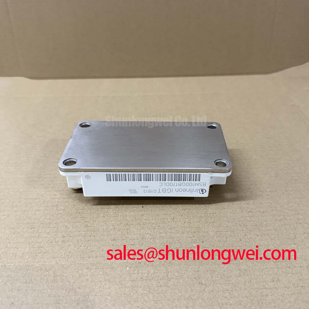
Benchtop Waveform Tuning: Mitigating Stress via Thermal Time Constants and Peak Junction on BSM100GB170DLC
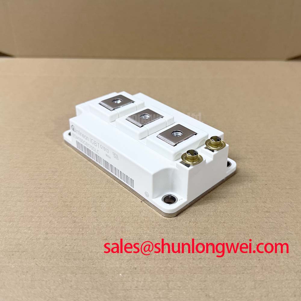
The 1700 V, 100 A ratings identify the principal electrical class of the BSM100GB170DLC, but they do not by themselves define an allowable operating point for a pulsed inverter, regenerative braking chopper, or photovoltaic central inverter. During a bench test, separate the steady state conduction loss from switching loss and pulse overload behavior. A thermal model should use the manufacturer’s published junction to case and case to heatsink data when available, with the actual baseplate interface, heatsink, airflow, duty cycle, and cooling control included in the calculation.
For short overload pulses, the case temperature may remain relatively stable while junction temperature changes more rapidly. An engineering calculation based on a multi RC thermal network can estimate the transient junction response, but the resulting peak remains system dependent. Engineers should correlate the model with thermocouple or infrared measurements taken at suitable reference points, while recognizing that surface temperature does not directly equal semiconductor junction temperature. Repeated pulse testing should be performed within the manufacturer’s stated safe operating area and switching conditions.
In a regenerative braking chopper, the module may transfer stored DC link energy into a braking resistor. The resistor’s pulse energy rating, chopper duty cycle, DC link voltage, and protection response determine the stress seen by the switching device. The BSM100GB170DLC rating should not be interpreted as a guaranteed braking resistor power rating. Confirm the energy balance, fault response, and thermal recovery time at the system level.
For a utility scale 1500 V high power central solar photovoltaic inverter, the 1700 V device rating can be considered only after the complete DC link transient profile is measured. Designers should verify switching overshoot, isolation coordination, creepage, clearance, surge protection, and control response under the most demanding operating conditions. The available Infineon IGBT Modules and Discretes portfolio provides a suitable manufacturer reference point for comparing official power semiconductor documentation, but product substitution requires a complete electrical and mechanical review.
Thermal interface preparation is also part of the test setup. Clean both mating surfaces, apply the selected thermal interface material according to its supplier process, and tighten fasteners in a controlled cross pattern using the equipment manufacturer’s specified torque. 💡 Bench Tip: Record the cold resistance and diode test observations immediately after ESD safe handling, because later comparison is more useful when probe pressure, temperature, meter range, and terminal contact method are kept consistent.
Preventing Spurious Faults: High Frequency Commutation Loop Inductance Guidelines for BSM100GB170DLC
During turn off, stray inductance in the commutation path converts current change into voltage overshoot. The relationship is commonly evaluated by considering the DC link voltage together with the inductive term created by loop inductance and current slew rate. This is an engineering calculation, not an additional factory rating of the BSM100GB170DLC. The measured collector emitter peak must be compared with the device voltage rating and the system’s protection limits using a properly compensated high voltage probe.
Minimize the physical area of the high current commutation loop and keep the forward and return conductors closely coupled. A laminated or symmetrical busbar arrangement may reduce parasitic inductance, but the suitable geometry is determined by current, insulation, mechanical spacing, switching behavior, and the complete inverter assembly. Do not apply a generic inductance target to this module without measuring the assembled circuit.
Snubber selection should follow measured ringing frequency, peak voltage, switching energy, and capacitor pulse current capability. A capacitor that suppresses one operating point may increase turn on loss or circulating current at another. The resistor and capacitor network should therefore be evaluated with double pulse testing and thermal measurement. If the circuit includes a freewheeling diode, reverse recovery behavior can add commutation current and electromagnetic interference; the diode characteristics, gate timing, DC link impedance, and busbar layout must be examined together.
For long motor cables, the cable and motor input impedance can create reflected wave behavior and additional terminal voltage stress. A suitable output filter, dv/dt control strategy, or cable termination approach should be selected from measured motor terminal waveforms rather than assumed from the module rating. This is especially important where a braking chopper, inverter bridge, or boost stage shares the same DC link.
When troubleshooting intermittent overvoltage faults, inspect probe grounding, sensor bandwidth, gate timing, busbar joints, capacitor connection length, and the physical return path before assigning the fault to the IGBT module. Compare the waveform at the module terminals with the waveform at the DC link capacitor. A difference between those locations may indicate commutation path inductance or measurement setup influence and should be verified under controlled switching conditions.
Field Diagnostics and Commissioning: Static and Dynamic Current Distribution in BSM100GB170DLC Topologies
Static current distribution should be checked after confirming identical electrical roles, compatible gate drive conditions, and a mechanically uniform thermal interface. The BSM100GB170DLC carries an official rated current of 100 A, but permissible continuous and pulsed current depends on junction temperature, switching loss, cooling, duty cycle, and the manufacturer’s detailed curves. When devices operate in parallel, designers should verify current sharing through measured collector emitter voltage, gate waveform comparison, thermal mapping, and current probe data.
IGBT conduction voltage generally changes with temperature and operating current, and this behavior can support static sharing in appropriately designed parallel arrangements. It does not remove the need for matched electrical paths. Equal conductor impedance, symmetrical gate wiring, controlled emitter reference routing where specified by the module documentation, and consistent thermal coupling are design considerations for dynamic balance. The final arrangement should be validated during turn on, turn off, overload, and fault interruption tests.
Commissioning should begin at reduced DC link energy with a current limited test source where practical. Verify gate to emitter behavior at the module terminals, not only at the driver output, because common impedance and inductive coupling can alter the actual waveform. Check that the gate driver supply sequencing, fault reset logic, desaturation or overcurrent protection, and dead time correspond to the selected control board and the applicable Infineon data.
For a central photovoltaic inverter, the DC link can receive energy from multiple power conversion paths. A boost stage, precharge circuit, braking chopper, and inverter bridge may interact during startup or grid disturbance. The BSM100GB170DLC should be evaluated within that complete topology. The system integrator should confirm whether the original design uses this part in a chopper position, bridge position, or another switching location before interpreting measured terminal behavior.
A neutral comparison candidate such as FF45017ME4 may be reviewed as a separate power module reference, but its voltage, current, gate characteristics, pin arrangement, thermal data, and mechanical interface must be checked independently. Similar package descriptions or current labels do not establish drop in compatibility.
Preventing Spurious Faults: Negative Gate Bias versus Active Miller Clamp Guidelines for BSM100GB170DLC
High dv/dt at one switch can couple through the opposing device’s Miller capacitance and disturb its gate to emitter voltage. The resulting behavior depends on gate resistance, driver impedance, commutation layout, device capacitances, DC link conditions, dead time, and measurement bandwidth. Active Miller clamping and negative gate bias are possible design approaches, but neither should be assigned a universal setting for the BSM100GB170DLC without the manufacturer’s gate drive limits and switching test results.
A low impedance gate loop reduces the opportunity for unwanted gate voltage displacement. Keep the outgoing gate path and return path short and closely coupled, separate high current commutation conductors from sensitive gate control wiring, and verify the driver reference at the module terminals. If an active Miller clamp is used, confirm its timing and current capability during the actual turn off transition. The clamp must not interfere with intentional turn on behavior or create excessive driver dissipation.
Negative gate bias can improve off state noise immunity in some high dv/dt topologies, but the appropriate value is system determined. Designers should verify the allowable gate emitter voltage range, driver isolation, startup sequence, fault reset state, and negative supply transient behavior from the official documentation. The commonly discussed negative bias range must not be treated as an official BSM100GB170DLC parameter unless it is explicitly stated in the applicable datasheet.
During commissioning, monitor both the commanded gate signal and the opposing switch gate signal while measuring collector emitter voltage with a correctly rated differential probe. If a fault appears only at high current or high bus voltage, compare the timing and amplitude of the gate disturbance with the commutation voltage transition. Check driver supply decoupling, isolation capacitance, gate resistor placement, and the return path before changing protection thresholds.
Reliability improvements should be validated with controlled double pulse tests, thermal observation, and fault interruption trials. Broader technology context for switching loss, parasitic behavior, and wide bandgap design tradeoffs is available in the Wide Bandgap Revolution engineering guide. Those principles are useful for circuit review, but they do not replace the official electrical limits for this Infineon module.