

Content last revised on September 25, 2026
F3L150R07W2E3_B11 Product Overview
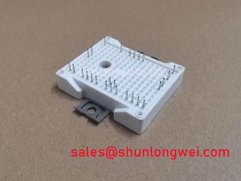
Before connecting the DC link, verify the nameplate boundary of F3L150R07W2E3_B11, inspect the power terminals for mechanical damage, and confirm that the original equipment documentation matches its 650 V and 150 A ratings. This Infineon IGBT module is identified in the supplied official product data as a PrimePACK package. The terminal arrangement, mounting pattern, gate connections, driver supply requirements, and switching limits must be verified against the original equipment documentation before a replacement is energized.
| Parameter | Specification Status |
|---|---|
| Product model | F3L150R07W2E3_B11 |
| Manufacturer | Infineon |
| Collector-emitter voltage rating | 650 V Official Specification |
| Current rating | 150 A Official Specification under specified conditions |
| Package category | PrimePACK Official Specification |
F3L150R07W2E3_B11 Circuit Protection and Reliability: Heatsink Contact Pressure and Surface Control
Start thermal work with the heatsink rather than the module. Remove residual thermal compound, oxidation, trapped dust, and hardened interface material from the contact surface. A flat, clean surface helps prevent local thermal resistance from dominating the module temperature rise. Where the service process specifies thermal interface material, its thickness should be controlled to provide coverage without creating an unnecessarily thick thermal path. A typical industry assembly reference is a thin, uniform thermal interface layer in the 50 to 100 μm range, but the final material type and layer thickness remain a Design Consideration determined by the heatsink flatness, interface material data, and equipment manufacturer requirements.
Baseplate curvature, heatsink machining marks, and uneven clamping can create air pockets that are not visible after assembly. During maintenance, inspect the transferred thermal material pattern after removal where practical. Areas with poor transfer can indicate uneven pressure, surface contamination, or a warped mounting surface. Correcting the contact condition is preferable to increasing cooling fan speed or altering protection thresholds, because those actions do not repair the heat path between the module and the heatsink.
Install mounting screws in a crosswise sequence and increase tightening progressively so that force develops evenly across the module base. The final torque must follow the applicable Infineon mechanical documentation and the original equipment assembly instruction. Do not assume that a torque value used on another housing, screw size, or heatsink design applies to this module. Terminal fasteners also require controlled tightening because a loose power connection can add resistive heating, while excessive mechanical force can damage threaded inserts or busbar interfaces.
Maintenance Note: Periodically monitor terminal contact temperature rise and verify that the cooling airflow path remains clear of dust accumulation and blocked filters.
For industrial inverter welders and medium frequency induction heating supplies, enclosure contamination can be as important as the electrical schematic. Conductive dust, metallic debris, condensation residue, and degraded thermal compound can change the practical stress seen by the power stage. Design Consideration calls for maintaining appropriate creepage and clearance around energized busbars according to the complete system voltage, pollution degree, enclosure construction, and governing equipment standard. The module rating alone does not establish insulation compliance for the finished machine.
Where a replacement decision includes a comparison with another module family, engineers can review the published details of BSM100GAL100D as a separate technical reference. Any interchange assessment should compare voltage class, current requirement, package footprint, terminal position, driver behavior, cooling arrangement, and protection settings. A similar current figure or a visually similar housing is not sufficient evidence of electrical or mechanical compatibility.
F3L150R07W2E3_B11 Operational Boundaries: Evaluating Auxiliary Emitter Return Paths
Gate drive stability should be checked at the module connection points with the actual power loop energized under controlled conditions. If the verified terminal drawing for the installed assembly provides a separate auxiliary emitter or Kelvin emitter return, route that return directly to the driver reference rather than allowing it to share the high current emitter path. This is a Design Consideration intended to reduce common emitter inductance influence during switching. The presence, label, and permitted use of any auxiliary terminal must be confirmed from the original module documentation; it should never be inferred from another Infineon housing style.
A shared return path can cause the gate voltage measured at the driver board to differ from the effective gate voltage at the module. Under load transitions, the high current loop creates voltage movement in parasitic inductance. That movement can disturb the intended turn on and turn off behavior, contribute to ringing, or make an otherwise stable driver appear inconsistent. Oscilloscope measurements should therefore include the relevant gate to emitter reference at the module, the collector emitter waveform, and the DC link response. Probe arrangement matters: long ground leads can add measurement artifacts that resemble actual oscillation.
Freewheeling diode commutation must also be observed in the installed topology. Reverse recovery behavior from the companion diode path can produce abrupt current transition conditions, while busbar geometry and DC link placement determine how much of that event becomes voltage overshoot or radiated noise. Snubber selection, if used in the original equipment, is a system level Design Consideration. It should be evaluated through measured switching waveforms and thermal checks rather than copied from an unrelated converter.
Engineers working on a rectifier stage or an associated high current conversion stage may also need to inspect the operating relationship with devices such as FZ800R12KS4_B2. This linked module is a separate product reference, not a prescribed substitute or companion for F3L150R07W2E3_B11. The DC link voltage, rectifier topology, fault energy path, and mechanical installation must be assessed as a complete assembly.
Negative gate bias, if present in an existing drive design, should not be changed solely because a module has been replaced. Gate voltage limits, isolation behavior, driver output capability, common mode noise, and desaturation protection coordination are system determined. During fault finding, compare the installed driver waveforms with a known good channel or documented commissioning waveform. A waveform difference may indicate gate loop imbalance, driver supply disturbance, measurement coupling, or a power loop issue, so it should not be assigned to one cause without verification.
Benchtop Waveform Tuning: Managing Transient Thermal Stress on F3L150R07W2E3_B11
When a power supply experiences pulsed overload, a steady state heatsink reading does not reveal the full junction temperature excursion. The thermal path responds over time, so short high energy pulses can elevate semiconductor junction temperature before the case and heatsink instruments show the same rise. The transient thermal impedance information in the applicable manufacturer documentation is the correct basis for evaluating this response. A multi RC thermal model can represent the changing junction to case response, but its inputs must come from verified device data and measured pulse conditions.
For bench evaluation, capture the current pulse profile, DC link voltage, switching waveform, case temperature trend, and cooling condition. The system engineer can then estimate peak junction margin from measured loss conditions and the applicable transient thermal data. This is an Engineering Calculation only when the switching losses, conduction losses, thermal impedance model, initial case temperature, and pulse duration are known. It must not be replaced by a generic overload multiplier or an assumed safe operating duration.
In inverter welder and induction heating equipment, pulse demand can change with process settings, workpiece coupling, output cable condition, and control response. A braking chopper and braking resistor, where included by the equipment manufacturer, manage regenerative energy by converting it to heat. Their resistor value, duty capability, thermal protection, and chopper control threshold are system specific. F3L150R07W2E3_B11 has an Official Specification of 650 V, so measured peak collector emitter voltage must be assessed against the actual DC link conditions and the complete switching transient, not against nominal bus voltage alone.
Long motor cables or transformer leads can create transmission line reflections that raise voltage at remote terminals. The voltage shape depends on cable length, impedance, load condition, output filter design, and switching edge rate. Design Consideration is to examine the waveform at the relevant equipment terminals and evaluate filtering where the system test indicates excessive reflected stress. Assigning a universal cable length, filter value, or overshoot allowance would not be technically valid for this product page.
The safe recovery window after an overload event also depends on the protection circuit, thermal state, cooling condition, and the nature of the load fault. Do not repeatedly reapply power after a protection trip without first checking the gate driver, DC link capacitors, heatsink contact, load insulation, and output stage for abnormal conditions. No field lifetime, failure rate, surge current capability, or overload endurance number is stated here because no verified product specific source has been provided for those values.
For broader context on where power semiconductor operating conditions are assessed across renewable energy, electric vehicle, and heavy industrial systems, see this technical resource on Industrial Applications. It provides application context but does not replace the product documentation and test evidence required for this specific module installation.
F3L150R07W2E3_B11 Circuit Protection and Reliability: Derating and Parallel Path Consistency
Where multiple switching paths operate in parallel, static and dynamic current sharing are separate checks. IGBT conduction behavior can exhibit a positive temperature coefficient in relevant operating regions, which can assist steady state sharing under controlled conditions. This is a Design Consideration rather than an assurance that parallel modules will share current safely. Actual sharing depends on device characteristics, gate drive timing, busbar symmetry, thermal coupling, emitter path geometry, and the operating point.
Dynamic imbalance usually appears first in switching waveforms. Unequal gate loop lengths, mismatched driver output impedance, unequal auxiliary emitter returns, and asymmetric busbar inductance can cause one path to switch earlier or experience greater voltage stress. Keep corresponding gate and power loop geometry as symmetrical as the physical layout allows, then verify the result through synchronized measurements under representative load. The system engineer should confirm peak current, collector emitter voltage, gate waveform, and temperature behavior for each path before approving a parallel arrangement.
Derating is not a fixed percentage that can be transferred from one converter to another. It is determined by the actual cooling system, switching frequency, load waveform, ambient condition, enclosure airflow, DC link behavior, protection response, and measured transient voltage. In maintenance work, compare the failed or suspect channel with an operating channel using the same measurement method. Differences in mounting pressure, terminal resistance, fan operation, gate drive waveform, or current sensor feedback can all influence apparent stress.
Infineon product families include specialized solutions with distinct qualification and integration scopes. The manufacturer’s information on Automotive Qualified Power Modules and Intelligent Power Modules should not be interpreted as a certification, qualification claim, or feature statement for F3L150R07W2E3_B11. For this module, procurement and repair teams should retain the equipment specific wiring records, driver settings, mounting instructions, and functional test results needed to establish a controlled replacement process.