


Content last revised on November 4, 2026
Preventing Spurious Faults: Reinforced Insulation Barrier Integrity and Guidelines for CM400DU-24NFJ
Before investigating nuisance gate faults, separate the module’s confirmed ratings from system-level insulation and transient-immunity requirements. The available product parameters establish a 1200 V voltage rating and 400 A current rating; they do not establish a reinforced-insulation withstand voltage or a common-mode transient immunity (CMTI) rating. Values such as an insulation test above 5 kV or CMTI above 100 kV/µs must not be attributed to this module without a manufacturer specification supporting them.
Design Consideration: Review the complete insulation coordination of the inverter, including the gate driver, isolation components, PCB spacing, busbar arrangement, enclosure, and test method. Keep conductive debris and residue away from insulation paths, and assess creepage and clearance using the applicable equipment standard, working voltage, pollution conditions, and material group. These distances are system design requirements, not a module specification inferred from its voltage rating.
When a fault appears only during switching, inspect driver supply integrity, isolation-barrier placement, and the return paths for gate and emitter signals. Use appropriately rated differential probes to compare the gate-to-emitter waveform with the switching event, and check whether common-mode movement coincides with unintended gate excursions. Mitsubishi Electric provides product-family information through its Power Semiconductors and High-Power Modules and Global Semiconductor Device Technologies pages; use the applicable device datasheet for model-specific electrical and insulation limits.
Benchtop Waveform Tuning: Main Terminal Alignment and Replacement Assessment
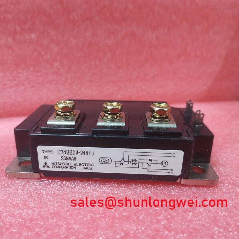
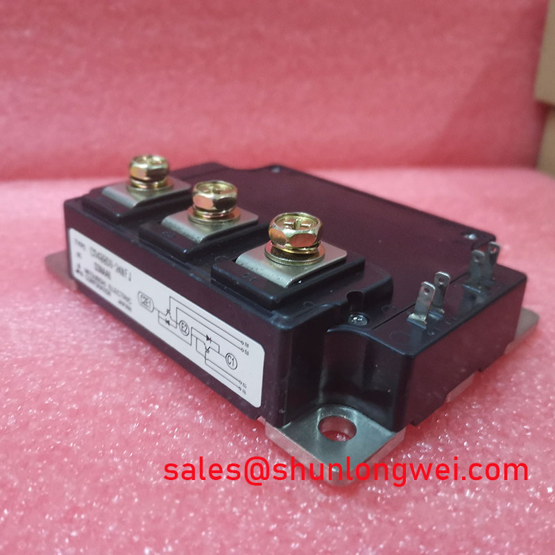
Check mechanical alignment before tightening the main terminals: the busbar or cable lug should sit flat on its contact surface without needing the screw to pull it into position. Confirm thread engagement, washer placement, and terminal alignment against the equipment assembly drawing and the module’s applicable mechanical documentation. Uneven contact or a misaligned conductor can impose mechanical load on the assembly and complicate interpretation of vibration-related or thermal-cycle faults.
For a replacement assessment, compare the documented ratings and mechanical interface of the installed unit with the candidate part. The CM450DX-24S1 is another module that may be evaluated against the equipment requirements; its name alone does not establish electrical, mechanical, or control compatibility. Verify pinout, package dimensions, terminal arrangement, gate characteristics, thermal interface, and the manufacturer’s specified operating conditions before considering substitution.
| Evaluation item | CM400DU-24NFJ | CM450DX-24S1 |
|---|---|---|
| Manufacturer | Mitsubishi Electric | Verify manufacturer documentation |
| Confirmed voltage rating | 1200 V | Consult the applicable datasheet |
| Confirmed current rating | 400 A | Consult the applicable datasheet |
| Package | Module | Verify mechanical documentation |
Bench Tip: Keep the module and test leads protected from ESD, and compare cold readings with a known-good reference taken using the same meter, polarity, and terminal mapping.
Switching frequency and cooling conditions affect losses and junction temperature, but no frequency-specific derating curve is established by the confirmed parameters above. Treat operation across a frequency range such as 2–16 kHz as a system evaluation, not a device guarantee: use the applicable switching-loss and thermal data, then validate case temperature and waveform behavior under the actual cooling airflow and load. High-speed rail and heavy freight locomotive traction inverters are potential compatibility contexts, subject to the traction system’s electrical, mechanical, and environmental requirements. For broader application context, see Industrial Applications.
CM400DU-24NFJ Circuit Protection: Gate Bias and Miller-Clamp Assessment
Assess unwanted turn-on by measuring the gate-to-emitter voltage of the non-commanded device during the opposing switch’s transition. A negative gate bias in the range of −5 V to −15 V, or an active Miller clamp, must not be treated as a prescribed setting for this module: neither value is established here as an official CM400DU-24NFJ specification. The driver design must remain within the gate-voltage limits and switching conditions stated in the applicable datasheet.
Design Consideration: A low-impedance clamp path can help control gate movement caused by Miller current, but its effectiveness depends on driver placement, emitter-reference inductance, gate-loop routing, and the module’s specified gate characteristics. Keep the gate and return paths compact, route them away from high-current switching loops, and confirm that the driver’s reference follows the correct emitter connection. Do not assume a pin assignment or Kelvin connection unless it is shown in the manufacturer’s terminal diagram.
When checking a suspected cross-conduction event, capture both gate signals and the relevant switching-node or current waveform with probes suitable for the common-mode environment. Compare commanded dead time and actual device transitions using the driver and system documentation. The fuse’s clearing behavior must also be coordinated with the inverter’s prospective fault current and the module’s documented short-circuit limits; select protection from the full system study rather than inferring a permissible fuse I²t value from the 400 A rating.
CM400DU-24NFJ Thermal-Electrical Optimization: Losses and Transient Evaluation
For pulsed operation, estimate junction temperature from the loss profile and the manufacturer’s transient thermal impedance data for the relevant pulse duration and cooling boundary. The confirmed 400 A rating alone is not a thermal model and does not define allowable overload duration, switching loss, or junction-temperature margin. Keep conduction and switching losses distinct in the analysis, and use the appropriate device curves and operating conditions.
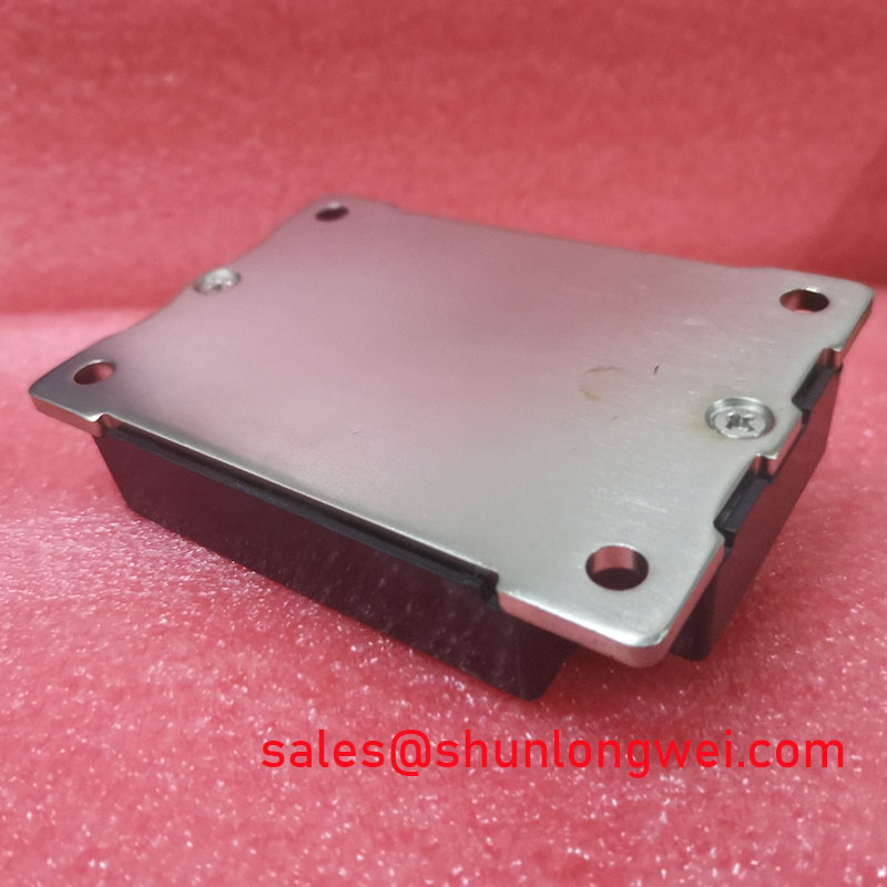
During bench work, record the case temperature, coolant or airflow conditions, load waveform, and switching behavior together; a temperature reading without its operating context cannot identify the source of excess loss. If measured behavior differs from the expected baseline, inspect the thermal interface and mounting flatness, then review gate timing and current sharing in the complete circuit. Avoid extrapolating a transient multi-RC model beyond the manufacturer’s published thermal data.
For inverter evaluation, minimize commutation-loop inductance as a design consideration and observe turn-off overshoot against the DC-link voltage using properly rated measurement equipment. The required margin depends on the module limits, bus structure, switching conditions, and protection strategy. Treat thermal response, surge coordination, and insulation as system-level verification tasks grounded in the applicable device documentation.


