

Content last revised on September 15, 2026
EVG31-050A Thermal Electrical Optimization: Fault Clearing Dynamics: Type I and Type II Desatur Practical Tuning
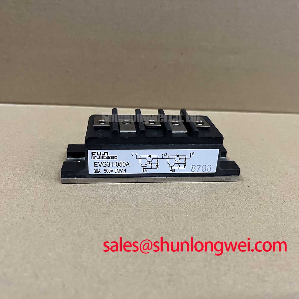
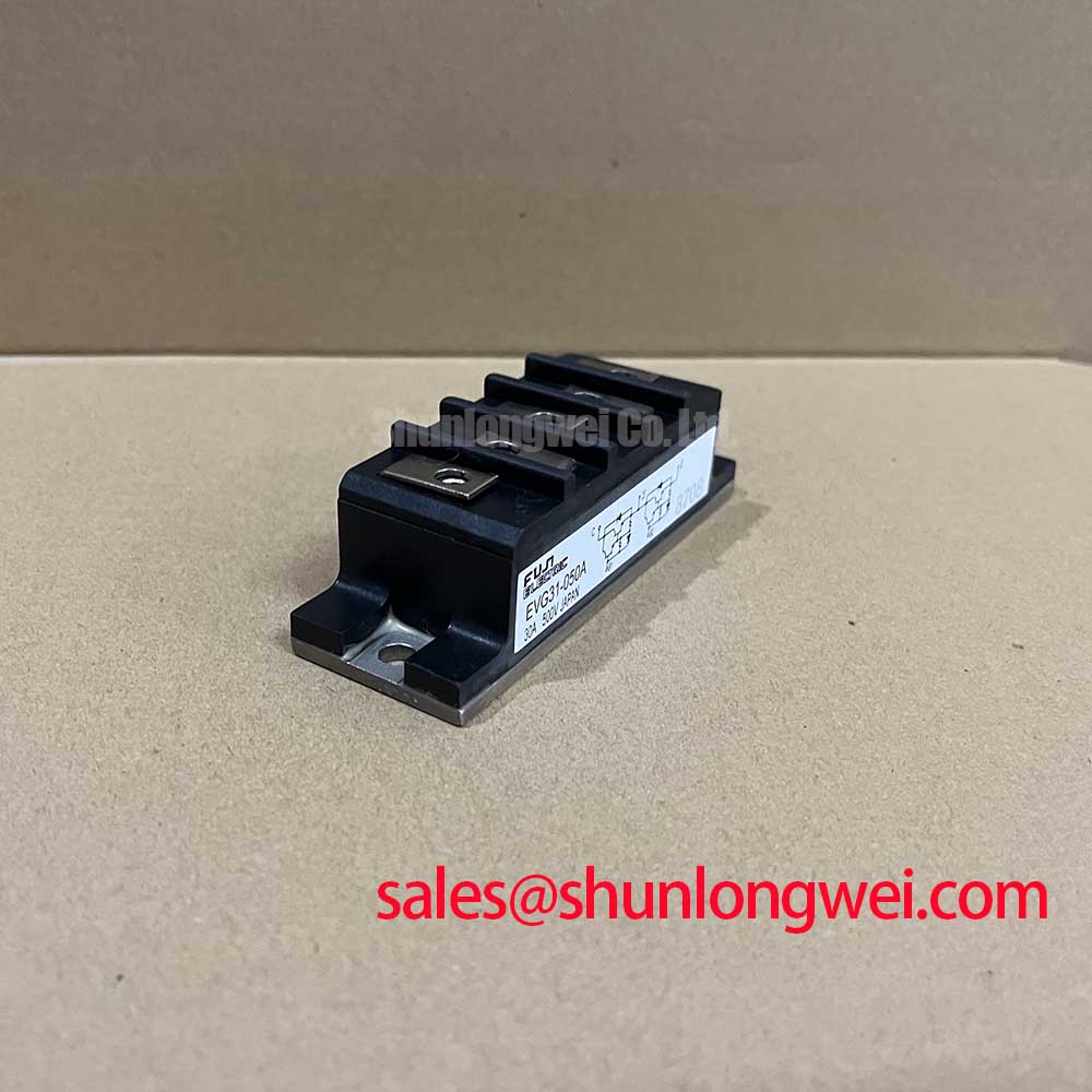
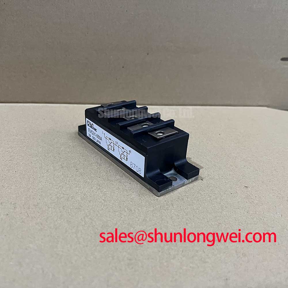
A desaturation protection check should begin at the gate driver rather than at the failed power device. Confirm that the sensing path, blanking arrangement, isolated driver supply, gate return, and fault reporting chain match the original control architecture. The EVG31-050A has a 450 V VCEO(sus) rating, so measured collector emitter voltage during normal switching and fault removal must be assessed against the actual DC link and observed overshoot, not against nominal bus voltage alone.
Type I and Type II desaturation terminology is often used differently across drive platforms. In practical work, the important question is whether the driver identifies a rising on state collector emitter voltage early enough to stop fault energy accumulation without forcing an abrupt current interruption that produces an excessive inductive voltage excursion. A protection response described as occurring within a given microsecond figure must only be claimed when it is documented for the installed gate driver and its complete sensing network. No short circuit withstand time or desaturation response time is listed in the provided EVG31-050A specifications.
Engineering Recommendation: use an oscilloscope with appropriately rated isolated measurement equipment to compare gate voltage, collector emitter voltage, phase current, and fault output during controlled commissioning. If an abnormal turn off waveform is found, examine the power loop and driver return path together. A long shared return or an unshielded desaturation sense lead can introduce noise that resembles a genuine fault or can delay recognition of one.
Two stage soft turn off is a system level protection method that can reduce the abruptness of current decay after a confirmed fault. Its suitability depends on the driver, bus inductance, clamp strategy, load current, and measured collector emitter excursion. The system engineer should validate peak voltage margin under representative switching tests, including the highest expected DC bus condition and the motor operating state that produces the most demanding current transition.
Busbar geometry is particularly relevant when the EVG31-050A is installed in a legacy drive. Design Consideration: keep outgoing and return current paths closely coupled to minimize parasitic loop inductance and suppress turn off inductive overshoot. Metal oxide varistors and other surge suppression elements should be inspected as coordinated parts of the DC bus protection network, with their clamping behavior and thermal condition verified in the original circuit context. They cannot be assumed to correct a layout induced switching spike by themselves.
💡 Pro Tip: Keep the positive and negative DC bus conductors physically paired through the switching loop, then verify the resulting turn off transient with a properly referenced measurement setup before accepting a repaired drive.
Assembly Integrity and Layout Architecture: Implementing Regenerative DC Bus Voltage Surge Dissipation for EVG31-050A
During motor deceleration, mechanical energy can return through the inverter into the DC link. Whether that energy is handled by a braking transistor and resistor, a shared regenerative unit, an active front end, or another arrangement is determined by the drive topology. The EVG31-050A official ratings identify its voltage, current, power dissipation, gain, and junction temperature limits, but they do not specify an internal braking switch, resistor value, braking duty, or allowable regenerative energy.
For a drive that uses a braking IGBT and ballast resistor, the braking path should be assessed from the motor deceleration profile, DC link operating range, resistor pulse capability, thermal recovery interval, protection threshold, and the switching device’s documented safe operating conditions. This is an Engineering Calculation and system verification exercise. It should not be inferred from the 30 A continuous current or 60 A peak current of the EVG31-050A alone.
Field troubleshooting should distinguish between a bus voltage rise that is expected during commanded deceleration and a rise associated with an unavailable braking path. Check the braking command signal, resistor continuity, mounting condition, wiring termination, and any recorded overvoltage events. A discolored resistor enclosure or open protective device may indicate that further testing is needed, but it does not establish a single cause without waveform and control evidence.
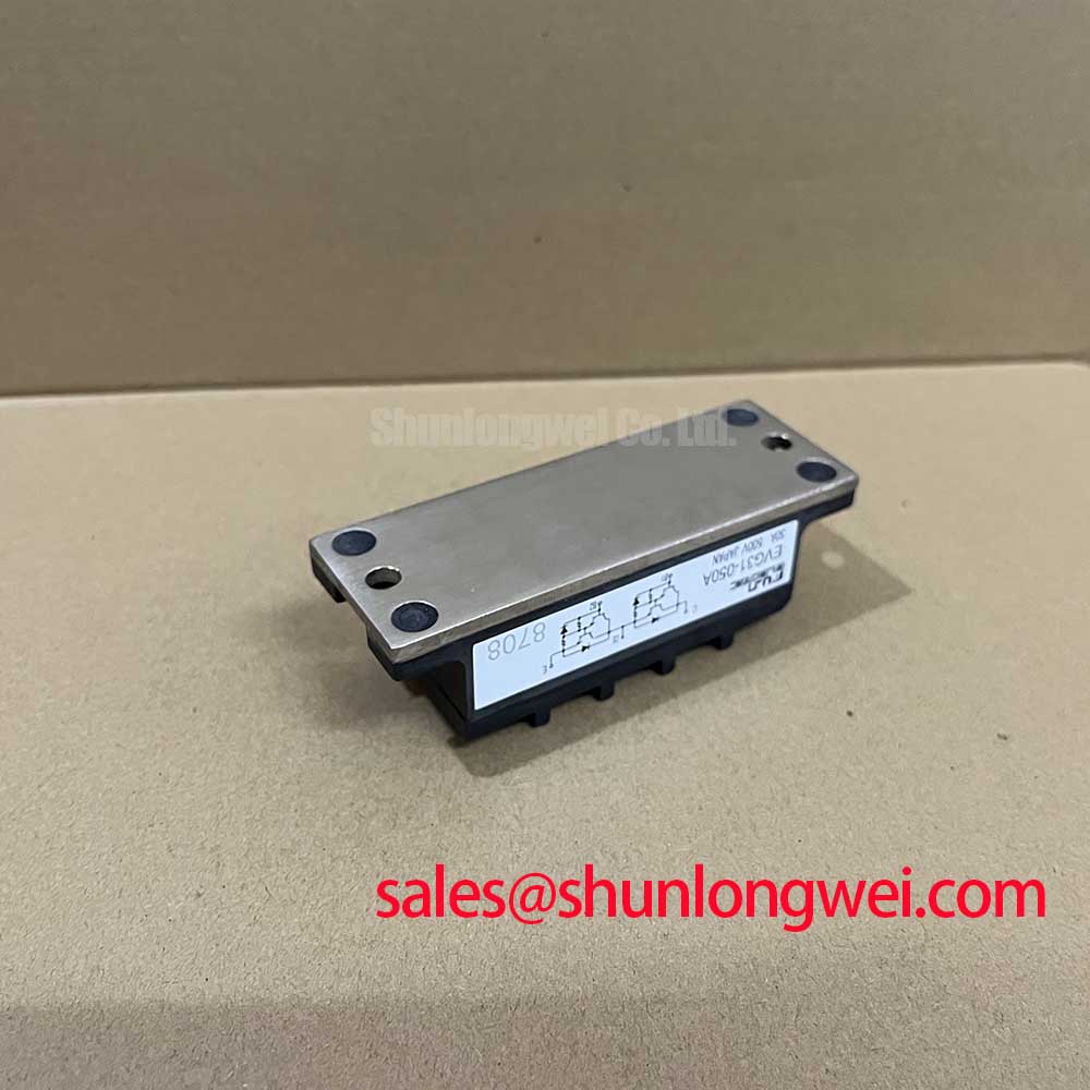
The thermal interface between the module baseplate and heatsink deserves the same attention as the braking assembly. Design Consideration: apply thermal interface material as a controlled thin film sufficient to fill surface irregularities while avoiding voids and excessive buildup. A 50 to 80 μm target range is a general industry mounting consideration, not an EVG31-050A factory thickness requirement. Use a cross pattern when tightening mounting screws so the baseplate settles progressively against the heatsink. The screw size, torque value, and torque sequence must be verified from the module mechanical documentation and the drive manufacturer’s assembly instruction.
Where a repair requires comparison with a different Fuji Electric power stage, the 3MBI50SX-120-02 can be reviewed as a separate module reference. Electrical ratings, circuit configuration, terminal arrangement, mounting geometry, gate drive requirements, and protection behavior must be compared before any replacement decision. It should not be treated as interchangeable solely because both devices are used in power conversion equipment.
EVG31-050A Operational Boundaries: Evaluating Baseplate Thermal Grease Layer Control Limits
Measure heatsink flatness, remove old interface residue without damaging the baseplate, and check that no burr, trapped washer, hardened grease ridge, or cable strain can tilt the module after tightening. The EVG31-050A is specified for a 150°C junction temperature. This is an Official Datasheet Specification, while the actual junction temperature in equipment depends on losses, heatsink performance, airflow, coolant condition where applicable, interface quality, ambient temperature, switching behavior, and load profile.
A grease layer that is too thick can add thermal resistance, while incomplete coverage or air pockets can create localized thermal stress. Design Consideration: a practical controlled grease film is often maintained within the broad 50 to 100 μm range when the relevant mechanical surfaces and material instructions support it. This general range is not a device specific guarantee. The correct process should be confirmed using the selected thermal compound documentation, module mounting drawing, and the original equipment maintenance standard.
Baseplate curvature and heatsink surface condition need to be assessed as a pair. Do not attempt to compensate for a visibly poor mating surface simply by adding more compound. Rework the mechanical interface as required by the equipment procedure, then tighten screws in a staged cross sequence. After thermal cycling, inspect the assembly for screw relaxation, grease migration, cable stress, and signs that the module has moved relative to the heatsink.
When evaluating unusual temperature rise, collect evidence from the cooling system before attributing the issue to the semiconductor. Verify fan operation, air path restriction, heatsink contamination, temperature sensor placement, load current, switching waveform, and the condition of mating inverter legs. The relationship between power loss and temperature is system dependent. The published 250 W power dissipation at Tc = 25°C is a datasheet condition and must not be read as a universal permissible dissipation figure in an installed drive.
For broader repair and test planning around thermal paths, enclosure cooling, and power assembly interfaces, The Advanced Thermal Management Revolution provides relevant technical background. Apply any general thermal principle only after verifying the EVG31-050A installation geometry and actual cooling arrangement.
Field Diagnostics and Commissioning: Common Mode Transient Immunity in Harsh Industrial EVG31-050A Topologies
Start commissioning with the motor mechanically safe, the DC link discharged according to the equipment procedure, and the control system checked for correct gate inhibit behavior. Common mode transients can couple through isolated gate drivers, current sensors, encoder interfaces, communication wiring, and measurement equipment. A spurious gate pulse may result from several interacting factors, including driver supply disturbance, shared emitter return impedance, inadequate isolation behavior, cable coupling, or controller timing. It should be investigated with synchronized waveform measurements rather than assigned to one cause.
No reinforced isolation rating above a particular kilovolt value and no common mode transient immunity rating above a particular kilovolt per microsecond value are provided in the EVG31-050A official parameters. Such values belong to the complete driver and isolation architecture, not automatically to the power module. The system integrator should obtain them from the installed driver, isolator, power supply, and safety documentation before making an isolation or CMTI claim.
Engineering Recommendation: separate sensitive control returns from high current switching paths, maintain intentional gate return routing, and evaluate shielding and isolation barriers under the actual cable and motor conditions. If negative gate bias is used by the original drive, retain only the documented driver arrangement and confirm its effect on turn off behavior, gate stress, and false triggering with measurements. Do not introduce a new bias value based on a generic module page.
Bootstrap supply performance also requires system specific verification. The high side supply capacitor, charging diode recovery behavior, PWM duty cycle, driver quiescent demand, and fault state all influence whether the high side gate remains correctly driven. Check the driver supply waveform at the driver pins using suitable isolated probing, especially during low speed operation, repeated acceleration, and fault recovery.
In rectifier and complementary power sections, the 6MBI15L-060 may be examined as a separate component reference when reviewing associated conversion stages. Its presence in a system does not establish compatibility with the EVG31-050A. Confirm circuit role, voltage class, current demand, mechanical format, control interface, thermal arrangement, and protection coordination from the equipment schematic and applicable component documentation.