

Content last revised on September 18, 2026
Preventing Spurious Faults: Atmospheric Neutron Radiation Impact on 12 Guidelines for EVK71-060
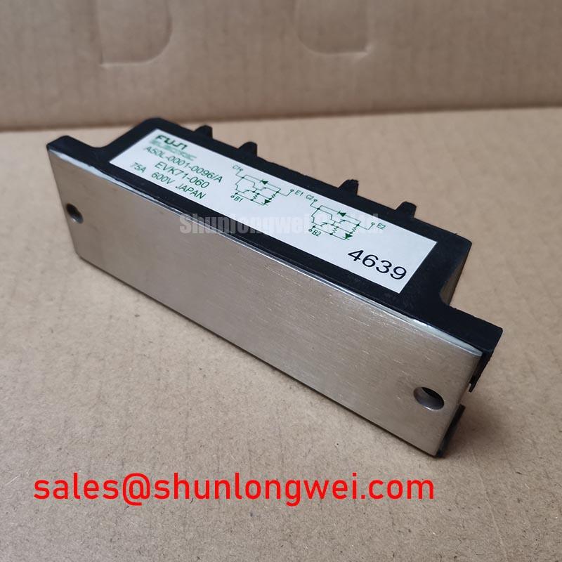
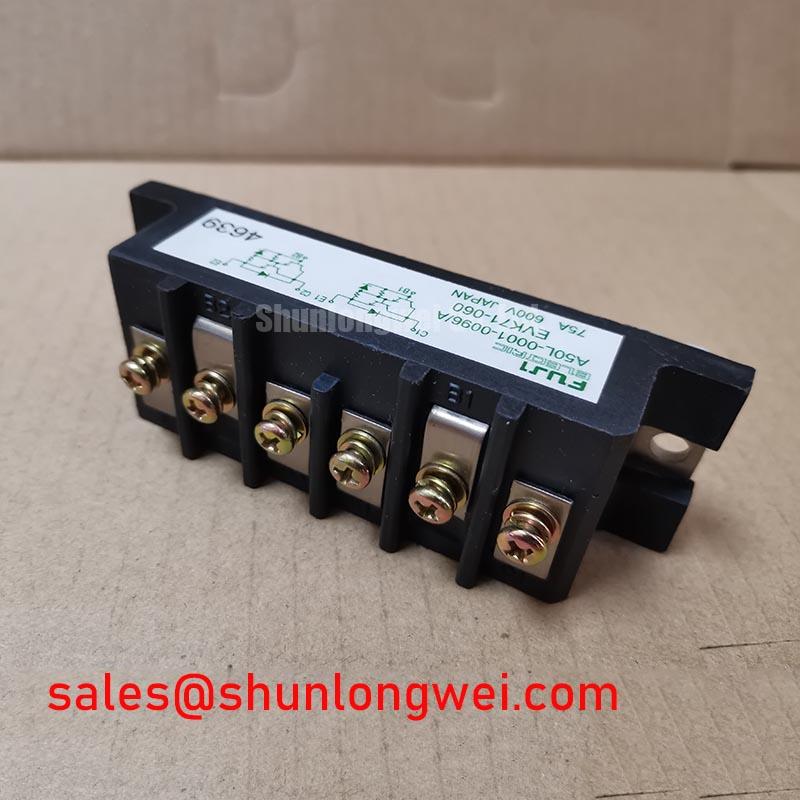
Begin incoming inspection by isolating the removed assembly, confirming the nameplate against EVK71-060, and recording its stated 600.0 V voltage rating and 80.0 A current rating before any electrical comparison. These are Official Datasheet Specifications for the Fuji Electric Fuji Power Module package. Verify the terminal map against the original equipment documentation before applying a meter, because the supplied product data does not establish the internal circuit topology, auxiliary terminal assignment, gate threshold, diode characteristics, or insulation test conditions.
With the circuit disconnected and stored energy discharged by the equipment’s approved procedure, use diode mode only as a comparative cold test between corresponding terminals on the removed unit and a known serviceable reference. Record polarity, reading stability, and any unexpected low resistance in both probe directions. A meter result by itself cannot establish switching health, but an asymmetric comparison can identify a reason to pause installation and inspect the connected driver, busbar, and load path.
💡 Bench Tip: Use ESD controlled handling and compare cold terminal readings only against the same verified circuit reference before reconnecting any gate drive cable.
Atmospheric neutron exposure and single event burnout are high risk reliability topics. No device specific neutron test result, FIT figure, altitude derating curve, or single event burnout limit has been provided for EVK71-060. It would therefore be inaccurate to calculate a failure rate, declare altitude suitability, or assign a DC bus derating value for this model. The 600.0 V rating is an Official Datasheet Specification, not a complete system transient or environmental qualification statement.
For equipment deployed at elevated sites, use a Design Consideration review that treats altitude, installed DC link voltage, switching transient magnitude, enclosure thermal conditions, grid disturbance history, and protection response as connected factors. The applicable product documentation and the finished equipment qualification plan should determine whether any environmental assessment is needed. The Fuji Electric Power Semiconductors Portal is an appropriate manufacturer resource for locating product family information and technical documentation.
A practical twelve point receiving and commissioning review can prevent false attribution of a field fault to radiation. Confirm the model marking, rated voltage, rated current, package contact condition, power terminal orientation, auxiliary terminal orientation, driver supply sequence, DC link polarity, protective earth continuity, controller fault log timing, oscilloscope probe reference arrangement, and the measured relationship between DC bus events and shutdown commands. These checks do not quantify neutron exposure. They establish whether an observable system event has a repeatable electrical signature.
When a converter trips without an obvious external overload, inspect recorded DC bus voltage, current command, gate drive status, temperature sensing path, and protection latch behavior together. A repeated shutdown that follows a particular operating transition may indicate a control, sensing, layout, or load interaction. It should be examined with the equipment schematic and a controlled waveform capture rather than assigned to one environmental cause. For commercial string inverter and micro grid energy storage evaluations, the system integrator should verify the site conditions and any required qualification requirements with the original equipment documentation.
EVK71-060 Circuit Protection & Reliability: Calibrating DC Link Capacitance Bank Layout and Low ES
Protection design starts by separating confirmed module data from converter level decisions. EVK71-060 is specified at 600.0 V and 80.0 A, while DC link capacitor selection, snubber implementation, busbar geometry, switching frequency, peak current, and protection thresholds are determined by the complete power stage. No official capacitance value, stray inductance value, short circuit withstand time, or desaturation threshold has been supplied for this module.
As an Engineering Consideration, turn off overshoot is related to DC bus voltage, commutation loop inductance, and current change rate. In ordinary circuit analysis, the inductive portion increases with loop inductance and changing current. This is why the capacitor bank and commutation conductors should be arranged to minimize the high current loop area, particularly when suppressing turn off overshoot. The final layout must be verified by switching tests that measure peak voltage against the installed DC link condition. A planar, symmetric conductor arrangement can be evaluated where the equipment architecture permits, but it is not an EVK71-060 factory requirement.
Capacitors located close to the power commutation path can reduce the portion of the loop shared by remote wiring. Their electrical characteristics under ripple current, temperature, aging, and mounting configuration remain system decisions. If a snubber is used, its value and damping behavior should be selected from measured ringing frequency and loss measurements on the actual assembly, not transferred from a different inverter layout.
Desaturation monitoring is commonly used as a Design Consideration in insulated gate power switch drivers, yet the sensing threshold, blanking interval, response sequence, and whether a controlled turn off sequence is appropriate must be validated for the exact driver and topology. A protection circuit that reacts too early can create nuisance trips, while one that reacts too late can expose the power stage to excessive energy. Review the driver data, the controller interlock logic, and the measured collector emitter behavior during representative fault tests performed under approved safety controls.
Gate drive return routing also belongs in the reliability review. Shared power return paths can introduce switching related disturbance into the driver reference and make a stable circuit appear intermittent. The engineering guide on Precision Gate Drive Design offers context for reviewing gate loop behavior, driver references, and measurement practice. For replacement assessment, 3MBI50SX-120-02 can be reviewed as a separate module record, but electrical ratings, package geometry, terminal arrangement, driver requirements, thermal interface, and original circuit compatibility must all be verified before any substitution decision.
Benchtop Waveform Tuning: Mitigating Stress via High dv/dt Cross Conduction Shoot Through on EVK71-060
Before energizing a repaired converter, verify that each command channel reaches the intended driver input and that the controller inhibits conflicting commands during startup, shutdown, and fault handling. The supplied EVK71-060 data identifies the voltage and current ratings but does not state a required gate drive voltage, a gate resistor value, a dead time, a Miller clamp requirement, or a permitted switching rate. Those settings must not be assumed from the module designation.
Cross conduction can occur when complementary switching devices are commanded on together or when switching disturbance changes the effective state of an inactive device. In a bench investigation, compare gate emitter waveforms, switch node voltage, DC bus voltage, and phase current using properly rated isolated measurement methods. Capture the event during the same operating transition that causes the alarm. A gate waveform that rises unexpectedly while its command remains inactive may indicate common source inductance, reference disturbance, coupling, probe setup error, or a driver fault. Verify the finding against a known good signal path before changing component values.
An active Miller clamp and a negative gate bias are common Design Considerations for controlling unintended turn on in some high switching stress circuits. They are not confirmed EVK71-060 requirements. The appropriate method depends on the driver’s ratings, insulation coordination, gate oxide limits stated by the relevant product documentation, and measured transient behavior. Designers should maintain short, controlled gate loop routing where practical and verify switching peak margins on the actual DC link. Dead time should be determined from measured switching behavior, device spread, temperature, and the controller’s timing resolution rather than selected as a universal fixed value.
For parallel paths, static current sharing and dynamic commutation sharing require separate checks. Positive temperature coefficient behavior is often discussed for power semiconductor operation, but its practical effect depends on the device family and operating condition. Do not infer equal sharing from identical command signals. Compare branch current behavior and thermal response under controlled load conditions, then review conductor symmetry, driver timing, and cooling contact consistency if the currents diverge.
Regenerative operating states deserve the same observation discipline. In systems using a braking chopper and resistor, the resistor energy capability, bus regulation logic, and chopper protection are system level functions. A DC bus rise may be associated with load regeneration, control timing, capacitor behavior, grid conditions, or another subsystem. Measure the event and follow the equipment schematic before associating it with the power module.
Field Diagnostics & Commissioning: Baseplate Convexity Compensation and Screw in EVK71-060 Topologies
Inspect the heatsink contact face and the module baseplate before assembly. Remove loose contamination using the approved service process, check for burrs or visible damage, and verify that the mating surface is flat enough for the equipment’s documented thermal interface procedure. The official information supplied here identifies a Fuji Power Module package but does not provide EVK71-060 baseplate flatness, mounting hole specification, screw size, mounting torque, thermal resistance, or allowable thermal interface thickness.
Thermal interface material is a Design Consideration rather than a module specific published value in the available data. Its purpose is to fill microscopic surface irregularities without creating a thick insulating layer. Use the original equipment manufacturer’s approved material, application method, and thickness control process. If baseplate convexity or heatsink flatness is suspected, compare the contact pattern after a controlled trial fit and correct the mechanical interface according to the equipment service documentation. Do not compensate for an uneven interface by applying excess material.
Fasteners should be tightened in a balanced sequence that progressively brings the module into contact across the full mounting face. The correct torque and sequence are determined by the mounting hardware, thread engagement, heatsink material, module drawing, and original equipment instructions. After tightening, inspect for uneven seating, displaced thermal material, damaged threads, or mechanical interference with power conductors and control wiring. Recheck cable strain relief so that busbar forces are not transferred into the module terminals.
Commissioning should begin at the lowest approved energy state with protective functions verified before normal load testing. Observe DC bus behavior, driver enable signals, cooling operation, and fault feedback while comparing them with the machine’s expected sequence. If temperature rise or intermittent faults appear, assess heatsink contact, cooling flow, electrical loading, switching waveform quality, and sensor feedback as separate possibilities. This preserves traceability for the EVK71-060 installation without claiming a diagnosis that the available official specifications do not support.