
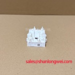
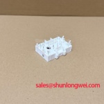
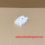
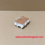
Content last revised on October 27, 2026
FP15R06YE3_B4 Operational Boundaries: Evaluating Long Motor Lead Reflected Wave Voltage Limits
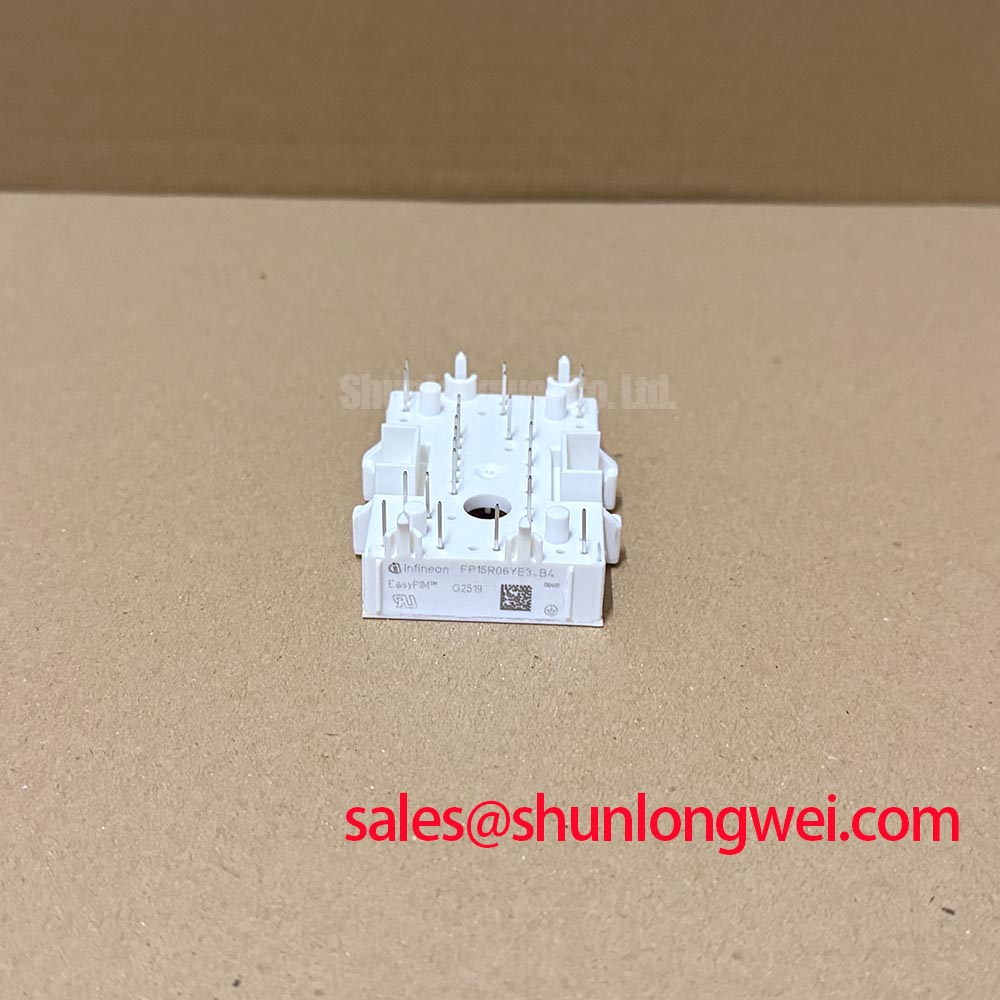
I first compare the inverter output waveform with the voltage measured at the motor terminals when investigating a drive that trips after a motor cable change. For the FP15R06YE3_B4, the 600.0 V rating establishes an electrical boundary for device evaluation; it is not a permissible motor-terminal pulse amplitude or a prescribed DC-link operating voltage. The 15.0 A rating also needs its datasheet conditions carried into the thermal and load assessment.
Design Consideration: A long motor lead behaves as a transmission line when its propagation time becomes significant relative to the inverter voltage transition. A mismatch between cable characteristic impedance and motor input impedance reflects part of the incident pulse. Under an idealized, strongly reflecting termination, the initial motor-terminal excursion can approach twice the incident voltage step. That relationship describes a transmission-line condition, not a guaranteed waveform produced by this module.
Separate motor-terminal reflected-wave stress from collector-emitter overshoot at the inverter. The former depends strongly on cable propagation and termination; the latter also involves the local commutation loop, switching behavior, and DC-link connection. Measuring only the motor terminals can therefore miss the voltage stress relevant to the semiconductor. Use appropriately rated differential measurement equipment, controlled probe routing, and consistent measurement locations when comparing the two.
Record cable length, cable construction, motor connection, operating load, and the conditions under which the unwanted ringing appears. Compare rising and falling transitions rather than relying on a single captured peak. A change in ringing after cable replacement can support an impedance-related investigation, but it does not by itself establish the cause of a module failure. Probe pickup, grounding arrangements, and changes in drive configuration deserve attention before drawing that conclusion.
Engineering Recommendation: Evaluate an output choke or dv/dt filter against the actual inverter, motor, and cable combination. Selection should account for pulse attenuation, motor current, switching conditions, losses, and the filter supplier’s application limits. An output choke and a dv/dt filter are not interchangeable descriptions, and their effects should be verified at the motor terminals. Preserve the equipment’s required electrical spacing when routing filter connections; adding a filter must not crowd power conductors against control wiring.
For compatibility assessment, light industrial automation and multi-joint robotic articulator drives are possible evaluation contexts, subject to the original power-stage requirements. When comparing repair materials, the FS30R06XL4 can be included in a documented component comparison, but should not be treated as a drop-in replacement for the FP15R06YE3_B4. Circuit topology, terminal mapping, switching behavior, mounting geometry, and cooling requirements must agree before a substitution decision is made.
Benchtop Waveform Tuning: Mitigating Stress via Baseplate Convexity Inspection on FP15R06YE3_B4
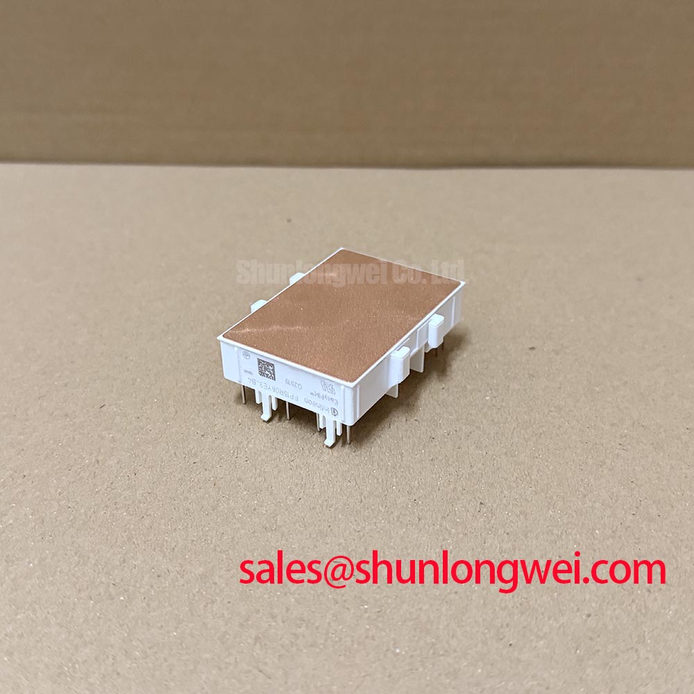
Inspect the heatsink contact surface and the module’s specified mounting interface before interpreting temperature-dependent waveform changes. A contaminated surface, damaged mounting feature, or mechanically loaded assembly can compromise thermal contact. The inspection should follow the package drawing rather than assuming that a visible curve indicates damage or that the module has a particular baseplate construction.
Design Consideration: Baseplate convexity is a package-specific mechanical characteristic, not a universal acceptance test. Do not infer a copper baseplate, allowable curvature, or flattening requirement from the generic Module package designation. Where the manufacturer specifies a curved mounting surface, assessment should use the stated inspection method and limits. Attempting to flatten the package against a reference surface can introduce stress instead of correcting the interface.
Clean the mating surfaces with a process compatible with their materials, then inspect for burrs, trapped debris, and damage around the mounting points. Apply thermal interface material using the package-specific assembly method. Coverage and bond-line control should provide a continuous thermal path without using excess material to compensate for an unsuitable heatsink. Neither a universal paste thickness nor a generic mounting torque is a verified specification for this product.
Where the mounting instructions call for staged or cross-pattern tightening, use a calibrated tool and follow that sequence. Support attached conductors so their weight or misalignment does not pull the module away from the cooling surface. After tightening, inspect the assembly for uneven seating and displaced interface material. Vibration restraint belongs in the surrounding mechanical design and should not rely on forcing a busbar into alignment through the module terminals.
Verify terminal functions from the circuit diagram before connecting the driver or power bus. Connector position and package resemblance are insufficient evidence of pin compatibility. Check that the assembled wiring preserves the equipment’s required creepage and clearance distances, including around fasteners, conductor edges, and control connectors. Account for the actual installation conditions rather than assigning a spacing rule from the voltage rating alone.
For a useful benchtop comparison, hold the electrical test conditions constant while investigating a mounting or cooling change. Correlate waveform captures with measured case or heatsink temperature and the equipment’s thermal model. A warmer assembly can alter switching behavior, but waveform drift alone does not quantify junction temperature or prove a defective thermal interface. Keep the mechanical inspection record alongside the electrical measurements so subsequent changes remain traceable.
Transient Dynamics & Electrical Design: Active Miller Clamp Implementation on FP15R06YE3_B4
Measure the off-state gate-emitter waveform during the complementary switch transition when investigating suspected parasitic turn-on. Place the measurement connections close to the relevant gate and emitter terminals, using equipment suitable for the common-mode transient. A waveform taken at the driver output can conceal disturbances introduced between the driver and the module.
Design Consideration: Collector voltage transitions couple displacement current through the gate-collector capacitance. If the gate discharge path has excessive impedance, the resulting voltage disturbance can reduce off-state margin. An active Miller clamp provides a local discharge path once its operating conditions are satisfied. Its usefulness depends on driver timing, connection inductance, clamp capability, and the surrounding circuit; it is not an inherent protection feature established by the FP15R06YE3_B4 model name.
Keep the clamp path and gate return compact, and avoid routing them alongside conductors carrying large switching currents. Where shared emitter-path inductance affects the gate reference, evaluate the resulting disturbance at the device terminals. Negative gate bias is another system-level option, but its value must remain within the module and driver limits, including transient excursions. A generic negative supply range is not an appropriate prescription for this part.
Engineering Recommendation: Keep the DC-link commutation path compact and geometrically balanced, then verify turn-off voltage margin with a controlled double-pulse test representative of the intended operating conditions. Evaluate the gate waveform, collector-emitter voltage, and current together. Apparent gate ringing can arise from measurement coupling as well as circuit behavior, while current spikes can include diode recovery and capacitive charging contributions. Those observations require correlation before identifying cross-conduction.
Review driver undervoltage behavior, interlocking, fault shutdown, and restart sequencing alongside the clamp circuit. A clamp does not replace coordinated protection. The IGBT Design & Integration guide provides broader context for evaluating gate-drive, thermal, and topology interactions without treating those system choices as module specifications.
Qualification claims also need a separate boundary. Infineon’s Automotive Qualified Power Modules resource concerns a manufacturer product category; it does not establish automotive qualification for the FP15R06YE3_B4. For repair release, retain the exact component identification, approved assembly instructions, protection settings, and measured switching results in the equipment record. Close the gate-drive investigation only after the observed off-state behavior and shutdown response meet the system’s documented acceptance criteria.