


Content last revised on September 17, 2026
Benchtop Waveform Tuning: Mitigating Stress via Multi Module Parallel Current Sharing on GD35PIX120C5SN_B90
| Manufacturer | StarPower |
|---|---|
| Product Model | GD35PIX120C5SN_B90 |
| Category | IGBT Module |
| Topology | Dual Half Bridge Module |
| Collector Emitter Voltage | 1200 V Official Datasheet Specification |
| Collector Current | 35 A Official Datasheet Specification |
| Package | Power Module |
| Series | Standard |
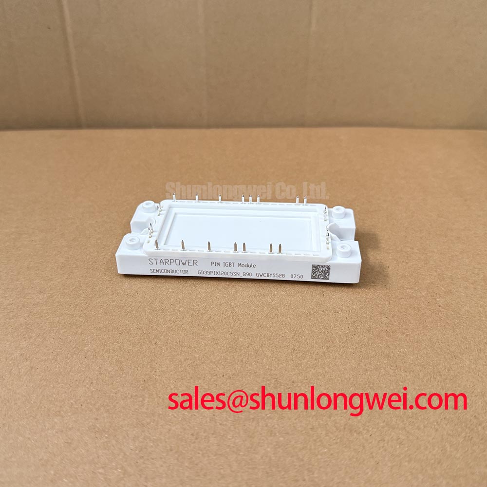
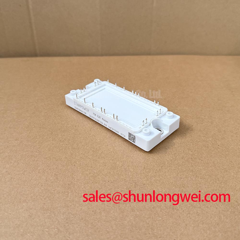
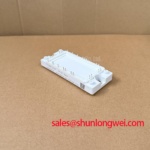
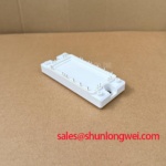
Measure the collector to emitter paths and gate related terminals with the drive cables disconnected, then compare each parallel branch for matching cold state behavior before energizing the DC bus. The GD35PIX120C5SN_B90 is a 1200 V, 35 A StarPower dual half bridge IGBT module, and parallel operation must begin with confirmation that every module location has the same topology, busbar orientation, gate driver reference, and protection routing.
For steady state sharing, IGBT modules can benefit from the positive temperature coefficient of collector emitter saturation voltage within relevant operating conditions. This is a Design Consideration, not a guaranteed current balancing figure for this specific module. It can help limit static sharing drift, but it does not correct an unequal gate loop, unequal cooling interface, or unequal power path resistance. A module that warms more quickly than its neighbor deserves investigation at the heatsink contact plane, terminal joint, and gate driver connection rather than an assumption that the semiconductor alone is responsible.
Capture collector emitter voltage and gate emitter voltage at each parallel location using a properly isolated measurement method. Compare turn on and turn off transition timing, ringing envelope, and the point at which desaturation or overcurrent protection responds. If one position shows a different waveform shape, inspect the physical conductor path first. Gate leads routed differently, separate return paths of unequal length, or a gate driver reference taken from a high current power return can create dynamic current imbalance even when static resistance checks appear similar.
Keep each parallel module’s DC link connection geometrically consistent and keep the commutation loops compact to suppress inductive voltage overshoot during switching. Clearance and creepage distances must be selected for the actual bus voltage, pollution conditions, enclosure material, and applicable equipment standard. The 1200 V rating is an official device limit, while the installed DC bus voltage and transient margin remain system level decisions that require oscilloscope verification under load.
For maintenance evaluation, technicians can document the terminal arrangement, mounting footprint, and driver interface before considering another part number. BSM35GD120DN2 can be assessed as a comparison candidate only after the original schematic, mechanical fit, terminal assignment, thermal interface, and switching behavior have been checked. It should not be treated as an automatic drop in replacement for GD35PIX120C5SN_B90.
GD35PIX120C5SN_B90 Thermal Electrical Optimization: Optimizing Gate Drive Loop Geometry to Pre Practical Tuning
Probe the gate emitter waveform at the module connection point while the bridge is switching, because a clean signal at the driver board does not prove a clean signal at the IGBT gate. Oscillation, unexpected gate voltage movement, or irregular switching edges can arise when the gate return shares impedance with the high current emitter path. The correction is a layout task: separate the sensitive driver return from the main switching current return wherever the module interface and driver architecture provide that option.
The official product facts establish a StarPower power module with dual half bridge topology, 1200 V collector emitter capability, and 35 A collector current rating. They do not establish a specific auxiliary emitter terminal arrangement, internal Kelvin connection, gate resistance, switching frequency, or driver voltage. The system integrator should verify the terminal designations from the original equipment documentation and the applicable module drawing before routing or modifying gate connections.
During freewheel commutation, reverse recovery behavior of the associated diode path can contribute to current transition sharpness and voltage ringing. A visible high frequency burst at turn on may involve diode recovery, power loop inductance, measurement pickup, or gate drive interaction. Use differential voltage measurement and current measurement together so that the observed waveform is tied to the actual commutation event. A snubber or MOV based overvoltage absorption network may be evaluated as a Design Consideration where measured transient energy requires it, but component selection must follow the switching waveform, DC bus conditions, repetitive duty, and system thermal test results.
⚠️ Field Alert: Isolate stored DC bus energy before removing gate or power connections, and tighten module hardware only to the equipment manufacturer’s specified fastening method with an even, thin thermal interface layer.
Radiated noise reduction starts with reducing loop area and avoiding long, separated outgoing and return conductors. This is not a claim of standalone EMC compliance. Device level layout work supports system testing, while compliance with equipment emissions requirements depends on the complete converter, enclosure, filters, cables, grounding arrangement, and test configuration.
Preventing Spurious Faults: High dv/dt Cross Conduction Shoot Through Guidelines for GD35PIX120C5SN_B90
Trigger on the opposite switch gate voltage and the half bridge output voltage when a protection trip occurs, then determine whether the inactive gate rises during the companion device transition. In a dual half bridge module, rapid collector voltage movement can couple through device capacitances and shared parasitic inductance. The result can be an unwanted gate excursion, cross conduction, abnormal DC bus current, or a protective shutdown that appears intermittent in normal service.
Use a dedicated low impedance turn off path and assess an active Miller clamp where the driver supports one. Negative gate bias is also commonly evaluated as a Design Consideration to strengthen off state immunity, but the actual bias range, clamp threshold, gate resistor values, dead time, and protection delay must be set by the gate driver design and verified against measured gate voltage limits. No drive voltage or timing value is specified here as an official parameter for GD35PIX120C5SN_B90.
Inspect the physical path between driver output, gate terminal, return terminal, and module mounting plane. A loose terminal, oxidized connector contact, cracked driver solder joint, or long return route can alter gate behavior under switching current even when a static multimeter check is inconclusive. Compare the suspect channel with a known healthy channel in the same equipment where possible. This avoids treating a single observed symptom as proof of one root cause.
Gate oxide stress is influenced by electrical field, temperature, switching events, and operating duration. The general mechanism of time dependent dielectric breakdown explains why gate voltage control and transient measurement matter, but it does not provide a service life prediction for this module. Avoid repetitive gate overshoot and verify the real operating waveform at the module terminals after any driver, wiring, or snubber change.
In light industrial automation and multi joint robotic articulator drives, this module may be evaluated where the original bridge design requires a 1200 V, 35 A dual half bridge power module. The evaluation must include the axis drive’s regenerative events, braking behavior, cable routing, motor inductance, and controller fault handling. A stable unloaded waveform alone is insufficient evidence of safe behavior during motion reversals or load changes.
GD35PIX120C5SN_B90 Thermal Electrical Optimization: DC Bus Operating Voltage Headroom Derating Practical Tuning
Record the actual DC bus voltage at the module terminals during regeneration, deceleration, supply disturbance, and intended maximum load, then compare the captured peaks against the 1200 V official collector emitter rating. Measurements should include switching transients rather than only the controller’s displayed bus voltage. The installed voltage headroom is determined by the converter topology, supply tolerance, motor energy return, bus capacitance, cabling, protective network, and measured overshoot.
Do not assign a numerical altitude derating, neutron induced failure rate, or single event burnout FIT value to GD35PIX120C5SN_B90 without a manufacturer specification or qualified test source for this device and use condition. Terrestrial neutron exposure and altitude are legitimate Design Considerations for high voltage power semiconductors, particularly when reduced atmospheric pressure and elevated DC bus stress coincide, but a specific prediction requires validated application data. Maintenance teams should instead document installation altitude, ambient temperature, measured bus transients, and fault history for the actual equipment.
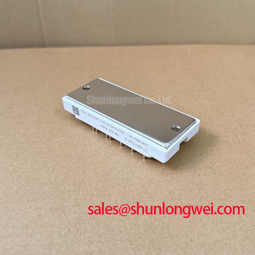
Thermal behavior should be checked through the complete heat path: module baseplate contact, thermal interface material coverage, heatsink flatness, mounting hardware condition, airflow or liquid cooling operation, and the load duty cycle. A localized temperature rise can reflect poor mechanical contact, uneven interface material, obstructed cooling, current imbalance, or a changing switching loss condition. Recheck electrical waveforms after correcting a mechanical issue because improved thermal contact can alter the operating point observed during a loaded test.
Use the equipment’s original insulation coordination requirements when reviewing exposed busbar spacing, terminal covers, connector routing, and enclosure contamination risk. These are system safety matters rather than published module certifications. For structured review of switching stress, thermal paths, and test priorities, the Power Electronics Masterclass provides a useful technical reference alongside the original drive documentation and measured bench data.