Content last revised on September 23, 2026
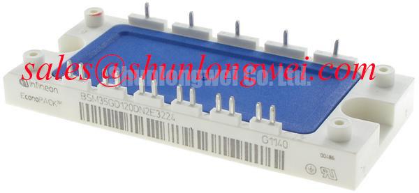
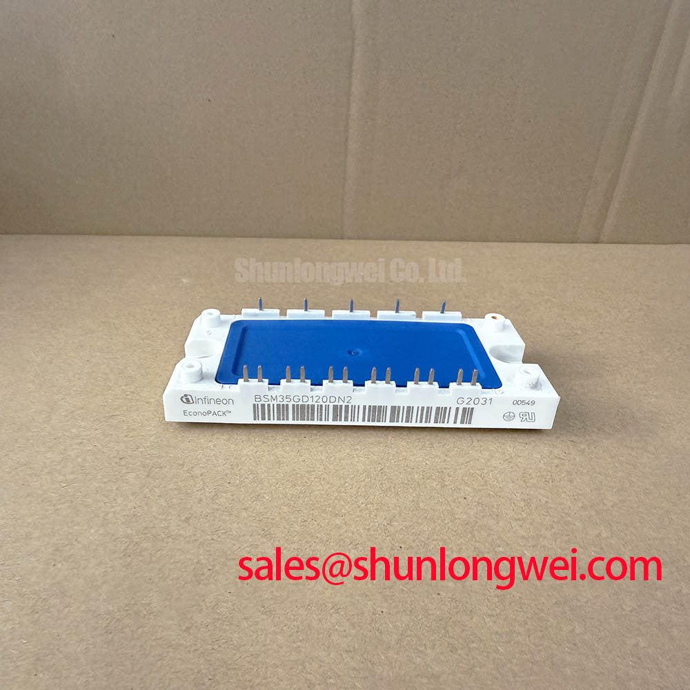
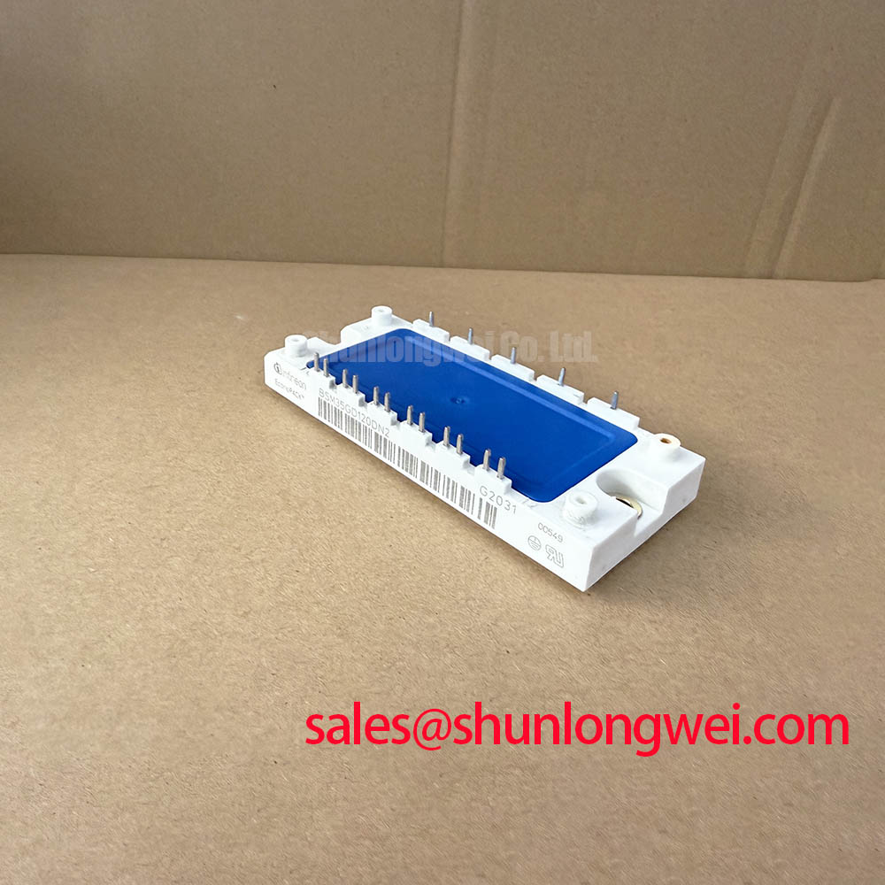
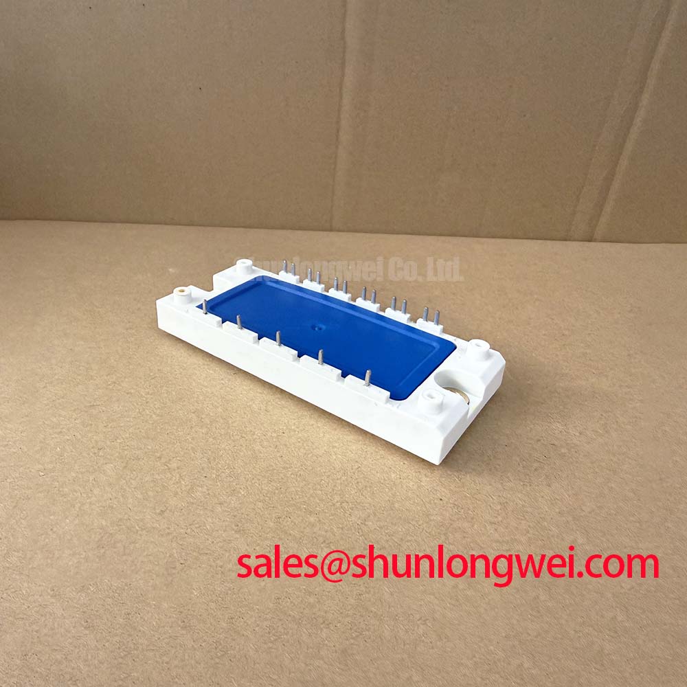
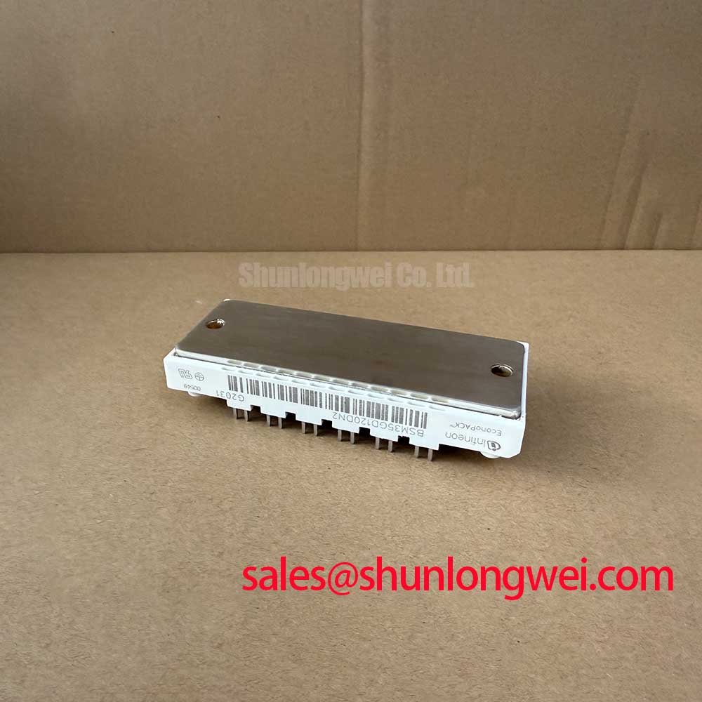
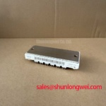
BSM35GD120DN2 Infineon 1200V 35A IGBT Module
Before installation, inspect the module body and terminals, confirm the nameplate rating, and perform a cold-state pin-to-pin check with the device isolated from every external circuit. The BSM35GD120DN2 is an Infineon IGBT Module rated at 1200.0 V and 35.0 A, with a module-style package. These are official product specifications; gate polarity, internal circuit topology, terminal assignment, switching data, isolation rating, and thermal limits should be confirmed against the applicable manufacturer documentation before energizing a replacement.
| Manufacturer | Infineon |
| Part number | BSM35GD120DN2 |
| Product category | IGBT Module |
| Rated voltage | 1200.0 V |
| Rated current | 35.0 A |
| Package | Module |
For incoming inspection, use an ESD-controlled bench and compare the cold resistance or diode-mode response of the tested unit with an approved reference device. A multimeter reading is useful for identifying an open circuit, an unexpected short, or a reversed measurement response, but it does not reproduce the dynamic voltage and current stress of an operating inverter. Do not interpret a single diode-test value as proof of switching performance. The Infineon IGBT Modules & Discretes Official Portfolio is a suitable manufacturer-level reference for confirming product-family information.
BSM35GD120DN2 Thermal-Electrical Optimization: Differential Gate-Source Loop Routing to Practical Tuning
Design Consideration: Keep the gate-drive return path physically associated with the corresponding emitter reference and separate it from the high-current emitter path wherever the actual module terminal arrangement permits. Shared copper can develop a transient voltage during fast current changes. The driver then sees a moving reference rather than the intended gate-to-emitter signal, which can produce ringing, delayed turn-off, or an apparent gate command that does not match the controller output.
For a compact industrial inverter or high-speed CNC spindle drive, inspect the complete gate loop from driver output to gate terminal and back to the driver reference. Minimize the loop area, avoid routing the gate trace alongside noisy DC-link or collector switching paths for long distances, and place the gate resistor or damping network according to the verified module and driver topology. The correct resistance is system-determined because it depends on the driver capability, gate charge, commutation inductance, switching frequency, and acceptable switching loss. Validate the result with a properly referenced oscilloscope measurement at the module terminals rather than only at the driver PCB.
When troubleshooting, first compare gate-to-emitter waveform shape at low-energy test conditions with a known-good assembly. Look for ringing that is synchronized with collector current commutation, uneven turn-on timing between parallel paths, or a gate signal that changes when the power return conductor is repositioned. These observations may indicate mutual coupling or measurement-reference error; they do not identify one single failed component without further testing.
The gate loop should also be checked after mechanical assembly. A busbar, shield, mounting plate, or replacement harness can alter the return path even when the schematic is unchanged. System integrators should verify creepage, clearance, insulation coordination, and probe placement against the complete equipment safety design. The related IGBT Design & Integration reference provides broader context for gate-drive, thermal, and circuit-topology evaluation.
Preventing Spurious Faults: Dynamic Braking Chopper Operation Guidelines for BSM35GD120DN2
In a DC-link braking circuit, the chopper IGBT and braking resistor must be evaluated together. During motor deceleration, stored mechanical energy can raise the DC-link voltage, while the resistor converts part of that energy into heat. The BSM35GD120DN2 official ratings of 1200.0 V and 35.0 A do not by themselves define the allowable pulse duration, repetitive braking duty, surge capability, or resistor rating. Those values must be established from the relevant electrical, thermal, and switching specifications and then checked against the actual drive profile.
Engineering Recommendation: Determine the braking resistor requirement from the motor inertia, deceleration command, speed range, DC-link voltage, braking interval, and thermal recovery time. The chopper current should be observed during the most demanding deceleration event, including abnormal stop conditions where the control system permits such testing. A voltage probe across the DC link and a current probe in the braking branch can show whether the protection threshold is being approached or whether the resistor is receiving a duty pattern outside its intended thermal envelope.
When modules are connected in parallel, static current sharing should not be assumed from identical part numbers. The positive temperature coefficient often associated with IGBT conduction can support sharing under suitable operating conditions, but busbar resistance, gate timing, thermal coupling, and wiring symmetry remain important. Use symmetrical collector, emitter, and gate-drive paths, and verify current balance during controlled switching tests. If a parallel arrangement is being considered as an alternative configuration, the BSM75GD120DLC can be reviewed as a separate reference product, not as an automatic substitute for this module.
The braking network may also include a MOV or another coordinated overvoltage clamp. Its voltage-current characteristic, energy capability, leakage, aging behavior, and coordination with the drive protection threshold must be assessed as a system. A MOV should not be selected from nominal DC-link voltage alone. The power stage designer should confirm the worst-case switching overshoot with the actual busbar and snubber arrangement, then verify that the clamp does not interfere with normal braking operation.
Assembly Integrity & Layout Architecture: Implementing Galvanic Gate Drive Isolation, Reinforced for BSM35GD120DN2
Galvanic isolation belongs to the complete gate-drive assembly rather than to the IGBT module rating listed above. For a reinforced-isolation design, verify the isolator, isolated power supply, PCB spacing, insulation system, transformer construction where applicable, and production test method as one barrier. Do not assign a specific isolation voltage or common-mode transient immunity value to the BSM35GD120DN2 unless it is stated in the applicable device documentation.
For a compact inverter, route the isolated gate supply and signal return so that the high dv/dt switching node does not capacitively inject a disturbance into the logic-side reference. Keep the isolation boundary clear of copper pours that bridge the barrier, control the placement of mounting hardware, and inspect the finished assembly for contamination or unintended conductive paths. The system integrator should verify the required clearance and creepage using the applicable working voltage, pollution environment, material group, and safety standard.
A start-up sequence should be tested before the DC link is applied. Confirm that the isolated driver supply reaches its validated operating region, that the gate output remains in the intended off state during undervoltage conditions, and that the controller reset behavior does not create a transient pulse. If the equipment uses a bootstrap supply, evaluate capacitor charging and discharging at the highest switching demand and check the associated diode recovery behavior from the selected circuit components. These are system-level design conditions, not confirmed specifications of this module.
⚠️ Field Alert: Disconnect the DC link and verify discharge before touching gate-drive connectors, because an apparently inactive inverter can retain hazardous energy in its bus and isolated supply circuits.
Trigger faults should be investigated with simultaneous measurements on the controller side, isolated driver output, and module gate-to-emitter terminals. Compare the timing relationship rather than relying on a logic probe connected to an undefined reference. If the fault appears only during high-voltage switching, inspect common-mode coupling, probe capacitance, isolation supply decoupling, and gate-loop routing before replacing the module. The BSM35GB120DN2 may be encountered in a related front-end or auxiliary power position, but its circuit role and ratings must be evaluated independently.
BSM35GD120DN2 Thermal-Electrical Optimization: Practical Limits for Reliability Evaluation
FIT calculations, single-event burnout assessment, cosmic-ray exposure, altitude derating, and service-life prediction require device-specific reliability data and the complete operating mission profile. No verified FIT value, neutron-flux failure rate, or operating-life figure is established here for the BSM35GD120DN2, so a numerical failure-rate claim would not be technically responsible. Engineers evaluating equipment above 2000 m should treat altitude, cooling performance, insulation coordination, and transient voltage margin as design-review subjects rather than applying an assumed universal derating factor.
For a high-speed spindle drive, record the actual DC-link voltage, switching overshoot, case temperature, heat-sink temperature, braking duty, and gate waveform during representative acceleration, steady-state, and deceleration cycles. Compare the measured peak collector-emitter stress with the official 1200.0 V device rating and apply the system safety margin required by the equipment design authority. The result should include measurement uncertainty, probe bandwidth, switching repetition, and the effect of enclosure temperature. A voltage margin that appears acceptable in a static test may change during regenerative braking or a fault-clearing event.
Thermal assembly should be checked at the same time. Clean both mating surfaces, apply the thermal interface material according to its manufacturer instructions, and tighten the mounting hardware using the equipment maker’s specified method. A generic torque value or TIM thickness must not be presented as an Infineon parameter for this module. After assembly, verify contact uniformity and observe case-to-heat-sink temperature behavior under controlled load.
Related power devices in the same cabinet can affect the module’s thermal cycle. A bidirectional DC-DC stage used for battery charging and discharging may impose alternating current direction, repeated power pulses, and enclosure temperature swings. The designer should model those cycles, check capacitor and resistor heating, and validate the resulting junction-temperature pattern with appropriate instrumentation. A front-end rectifier or auxiliary stage may use a device such as BSM75GB120DN2, but thermal interaction does not establish interchangeability.
For procurement and repair review, record the exact part number, rated voltage, rated current, package, terminal layout, driver compatibility, cooling interface, and measured operating waveform in the equipment service record. Final acceptance should be based on the verified documentation and controlled system testing rather than on the 1200 V and 35 A ratings alone.