

Content last revised on October 30, 2026
FP100R12KT4 Incoming Inspection and Measurement Checks
- With the DC link discharged and verified safe, match the FP100R12KT4 terminal markings to the circuit drawing before measuring rectifier, inverter, or brake paths.
- Record cold diode-mode readings with consistent probe polarity, gate conditions, and instrument settings; compare equivalent paths against a documented reference.
- Inspect the mounting surface, thermal interface, terminal connections, and driver return routing before applying power.
- Separate module insulation checks from gate-driver isolation checks, using the approved test procedure for each assembly.
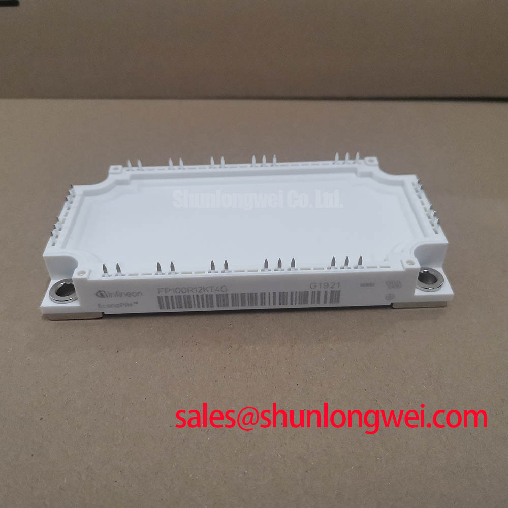
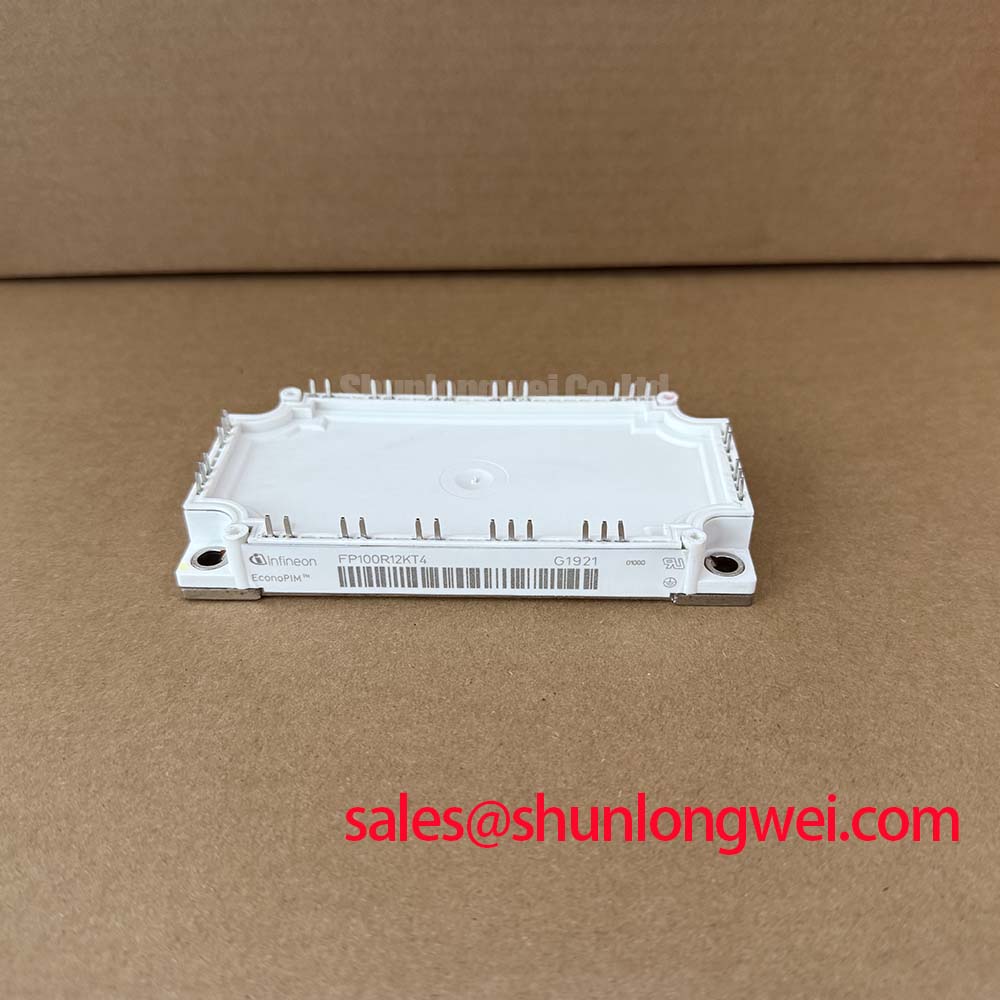
The Infineon FP100R12KT4 combines a rectifier, brake chopper, and three-phase inverter in an EconoPIM™ 3 power integrated module. Incoming inspection should distinguish these circuit sections before interpreting resistance or diode-mode measurements. A reading through the assembled power board can include charging paths, discharge resistors, and connected driver circuitry, so record the measurement configuration alongside the result.
💡 Bench Tip: Use ESD protection and compare cold measurements with the gate held at emitter potential under the approved test procedure, because an unintentionally charged gate can change the observed conduction state.
| Parameter | Official Specification |
|---|---|
| Model | FP100R12KT4 |
| Manufacturer | Infineon |
| Collector-emitter voltage, VCES | 1200 V |
| Continuous collector current | 100 A at case temperature TC = 80°C |
| Typical collector-emitter saturation voltage | 1.90 V at IC = 100 A, VGE = 15 V, and Tvj = 125°C |
| Package | EconoPIM™ 3 |
| Topology | PIM: rectifier, brake chopper, and three-phase inverter |
| Additional integration limits | Consult Datasheet for terminal assignments, thermal impedance, switching conditions, mounting requirements, and insulation test conditions. |
FP100R12KT4 Thermal-Electrical Optimization: Transient Thermal Impedance and Practical Tuning
Capture the load pulse, switching activity, and case-temperature measurement location before estimating peak junction temperature. As a Design Consideration, short overloads require the transient junction-to-case thermal response; steady thermal resistance alone does not describe the temperature rise during a changing load. Keep inverter, brake, and rectifier dissipation associated with their respective circuit sections rather than assigning all measured input loss to one semiconductor junction.
An Engineering Calculation can represent the datasheet transient response with a fitted multi-RC thermal network, then apply the time-dependent device loss to estimate junction-temperature rise above the case. Fit the network to the published response over the pulse durations relevant to the equipment. For repeated pulses, carry the residual thermal state into the next pulse. Resetting the model between pulses would hide accumulated heating and overstate the available temperature margin.
The official 1.90 V typical saturation-voltage point describes conduction at 100 A, 15 V gate-emitter voltage, and 125°C junction temperature. It provides a useful reference for loss assessment under those conditions. A practical calculation should also account for current waveform, duty cycle, switching losses, and diode conduction. Compare the resulting peak temperature with the applicable operating boundary using a case-temperature measurement that represents the installed thermal path.
As an Engineering Recommendation, check heatsink flatness, surface cleanliness, and the thermal-interface application before attributing unexpected heating to electrical losses. Follow the module mounting instructions for interface material and tightening sequence. Uneven contact can produce a local thermal restriction that an average heatsink reading misses. Thermal grease thickness and mounting torque belong to the approved assembly specification; arbitrary workshop values can change the contact condition.
For compatibility assessment, an industrial inverter welder or medium-frequency induction-heating supply requires evaluation of its actual switching topology, pulse loading, and cooling arrangement. The integrated three-phase inverter does not establish suitability for every resonant or welding converter. If external module paralleling is contemplated, designers should evaluate static conduction sharing and dynamic switching sharing separately; matched ratings alone cannot establish equal current distribution.
Preventing Spurious Faults: Assessing Contact Oxidation and Connection Heating in FP100R12KT4 Assemblies
Locate the hot connection on the assembled current path before assigning a contact-resistance requirement to the module. As a Design Consideration, external bolted busbar joints, board connections, and the module interface require different inspection methods. Identify which joint the measurement includes, then place separate current and voltage leads so that lead resistance does not dominate the result.
A four-wire micro-ohmmeter can support comparison of accessible power connections when the assembly is isolated and the test current is appropriate for the connected circuitry. Record probe locations, surface condition, and temperature. Use the equipment manufacturer's acceptance criteria instead of imposing a universal micro-ohm threshold. An elevated reading can justify inspection for contamination, loose hardware, damaged mating surfaces, or connection deterioration without establishing a single cause.
Thermographic inspection becomes more informative when equivalent connections carry comparable current and have reached comparable operating conditions. Account for surface emissivity and reflected heat before interpreting apparent temperature differences. Correlate a hotspot with voltage-drop measurements and load history. Tightening a warm connection without checking its specified assembly procedure can leave the underlying contact problem unresolved.
As an Engineering Recommendation, assess switching-frequency changes through their effect on total loss and cooling demand. Increasing switching activity can increase device heating even when output current remains unchanged. Restricted airflow, warm inlet air, or contamination of the heat exchanger can reduce thermal headroom. Establish the operating envelope from the measured assembly response and the device loss model, with attention to the hottest relevant semiconductor section.
The PIM topology also matters during repair procurement. The FP35R12KT4 is a related part for a documented comparison, with terminal mapping, current capability, thermal behavior, and driver compatibility assessed before any substitution decision. In a wider converter architecture, the FS200R12PT4 provides a separate inverter-module comparison; it should not be assigned the rectifier role simply because it appears elsewhere in the power chain.
FP100R12KT4 Operational Boundaries: Evaluating Current Tails and Switching Oscillations
Observe diode commutation current and collector-emitter voltage together when investigating ringing around an inverter switching transition. As a Design Consideration, diode reverse recovery interacts with commutation-loop inductance and the incoming switch's turn-on behavior. Reverse-recovery peak current and recovery abruptness depend on operating conditions, so a waveform captured at light load cannot establish the behavior at the intended hot operating point.
Separate the IGBT turn-off current tail from oscillation caused by the surrounding circuit. Probe placement, measurement-loop pickup, and instrument bandwidth can influence the apparent ringing. Compare measurements at consistent operating points and use probes suited to the voltage and transient environment. A change in the recorded trace after moving the probe return can indicate a measurement contribution that needs resolving before modifying the circuit.
As an Engineering Recommendation, review the turn-on gate-resistance network when recovery-related current stress is excessive. Slowing the transition can alter recovery stress while increasing switching loss. An RC snubber can modify ringing but adds its own dissipation and layout constraints. Determine either approach from measured waveforms and thermal performance, keeping the snubber current path close to the circuit it is intended to damp.
Dead time should accommodate driver propagation behavior and device switching behavior across the operating envelope. Insufficient separation can permit overlapping conduction; excessive separation can increase diode conduction and affect output behavior. Evaluate both gate signals at the device reference points and correlate them with the switching-node waveform. The controller setting alone does not reveal the timing that reaches the power terminals.
Desaturation protection needs a separate review of sensing delay, blanking, detection behavior, and controlled shutdown. The published typical VCE(sat) value is a conduction characteristic, not a ready-made protection threshold. As a Design Consideration, coordinate the driver response with the device short-circuit operating limits and the equipment fault sequence. Soft turn-off should control fault-current interruption without allowing the protection sequence to exceed those limits.
The system discussion in Peak Efficiency in Solar and Energy Storage offers broader topology context for reviewing commutation paths. Apply those concepts to the actual FP100R12KT4 schematic rather than transferring switching assumptions between different converter arrangements.
FP100R12KT4 Operational Boundaries: Evaluating Gate-Driver Common-Mode Transient Immunity
Check the gate driver's isolation and common-mode transient immunity against the measured switching-node behavior before investigating an unexplained gate pulse as a module fault. As a Design Consideration, driver CMTI describes the driver's response to rapid common-mode voltage changes. It is distinct from the power module's insulation test rating, and neither characteristic establishes the complete assembly's reinforced-insulation status.
Review the isolation barrier across the driver, isolated power supply, board spacing, connectors, and mounting arrangement. Clearance and creepage requirements depend on the applicable equipment standard and installation conditions. Apply dielectric testing only through the approved assembly procedure, accounting for circuitry connected across the test boundary. Insulation performance should be assessed under its stated test conditions rather than inferred from the collector-emitter voltage rating.
Inspect the gate-emitter waveform with a measurement arrangement that preserves the local reference. Coupling through parasitic capacitance, shared return impedance, and driver supply disturbance can contribute to unintended gate activity. As an Engineering Recommendation, shorten the relevant drive loop, review return routing, and evaluate the driver's off-state control using the complete switching waveform. Any layout or damping change should be checked for its effect on switching loss and protection behavior.
If the surrounding driver uses a bootstrap supply, evaluate charge replenishment during the actual switching sequence. Long high-side conduction intervals, startup conditions, and protection states can change the available supply margin. Assess capacitor discharge, driver consumption, charging-path impedance, and bootstrap-diode behavior together. Supply droop should be correlated with the gate waveform before assigning it as the cause of intermittent switching.
Infineon's EconoPACK™ Plus and CIPOS™ Nano IPM Series describe distinct product families; their package, integration, and protection features should not be transferred to this EconoPIM™ 3 PIM. For the installed FP100R12KT4, finish the gate-disturbance check by correlating command input, driver output, local supply, and switching-node transitions through startup, normal operation, and controlled fault recovery.