
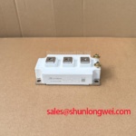
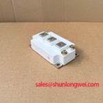
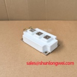
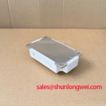
Content last revised on September 17, 2026
Preventing Spurious Faults: DC Bus Layout Guidelines for GT300HF120T2VH
| Model | GT300HF120T2VH |
|---|---|
| Brand | Industrial Manufacturer |
| Category | Power Semiconductor |
| Package | Module |
| Topology | General Power Stage |
| Series | Standard |
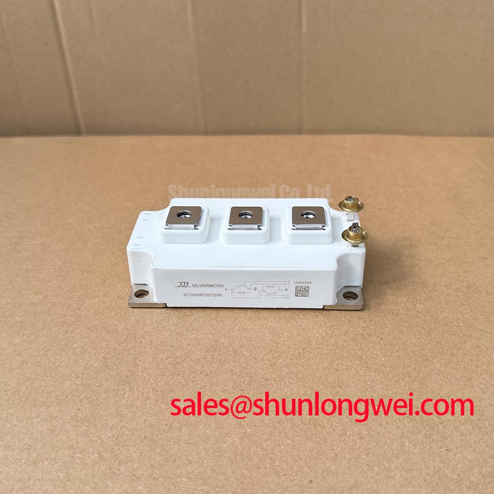
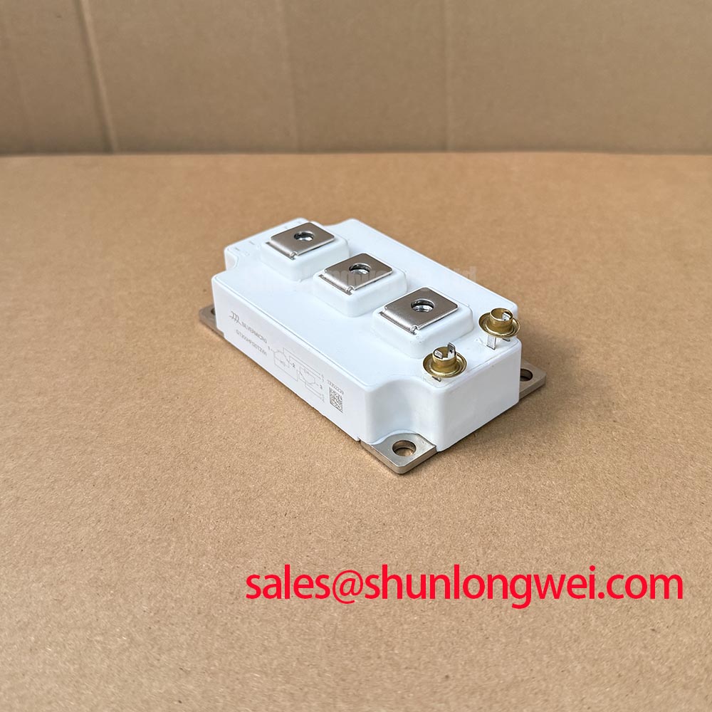
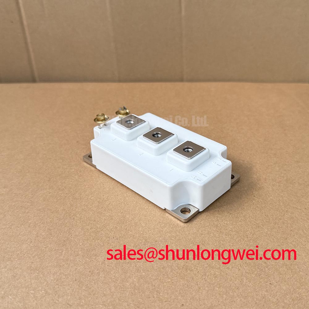
Probe the DC bus directly at the module connection points and compare the switching waveform with the DC link measurement to identify overshoot, ringing, or an unexpected gate disturbance. The GT300HF120T2VH is specified as a Power Semiconductor in a Module package with a General Power Stage topology, so the actual operating voltage, current, gate drive limits, terminal assignment, and switching limits must be taken from the equipment schematic and the applicable original technical documentation before commissioning.
A ringing waveform is not proof of a module defect by itself. It can arise from the physical loop formed by the DC link capacitor, busbar, module terminals, snubber network, and measurement probe ground lead. As an Engineering Calculation, the switching peak is influenced by the DC bus voltage plus the stray inductance multiplied by the rate of current change. This relationship explains why a short, wide, closely coupled current path is valuable when suppressing turn off overshoot.
Design Consideration: keep the positive and negative DC conductors physically close and geometrically symmetric across the power path. A laminated busbar or closely stacked planar conductor arrangement can reduce loop area when the capacitor and module placement permit it. The system engineer should validate the resulting peak voltage at the actual switching current, DC bus condition, temperature, and operating frequency rather than treating a layout rule as a universal guarantee.
When troubleshooting intermittent overcurrent trips in a commercial string inverter or micro grid energy storage converter, inspect the DC link capacitor connections, power terminal contact surfaces, busbar flatness, and the path between the local capacitor and the module. Loose hardware, oxidized interfaces, unequal conductor paths, and a long snubber connection can each alter the measured transient response. Repeat the test with the same probing arrangement because a long oscilloscope ground connection can introduce misleading ringing.
A snubber network is a system level transient control element, not an inherent published characteristic of this module. Designers should select its location, capacitance, resistance, voltage rating, pulse capability, and thermal behavior from measured switching data. The operating principle of transient energy control is described in this snubber circuit reference. Verify that any added network changes the full switching waveform rather than only reducing a visually prominent ringing frequency.
Field Alert: Isolate the DC link and confirm stored energy has been discharged through the equipment approved procedure before removing any power connection or changing an oscilloscope probe position.
GT300HF120T2VH Thermal Electrical Optimization: Fault Clearing and Desaturation Review
Capture collector or power node voltage, gate command, gate return, fault output, and DC bus voltage on the same time base when a protection event occurs. A fault event must be examined as a sequence: command state, current rise, detection decision, turn off behavior, bus response, and controller recovery. A single fault flag does not identify whether the initiating condition was load current, a gate command issue, busbar ringing, driver supply behavior, or a sensing path problem.
The official product information identifies GT300HF120T2VH as a module but does not provide a published desaturation threshold, short circuit withstand time, gate voltage range, current rating, or voltage rating in the supplied specification. Those limits must not be inferred from its model name. The gate driver protection threshold and timing must instead be checked against the module documentation used by the original equipment manufacturer and against measured behavior in the actual assembly.
Design Consideration: desaturation protection should respond to a sustained abnormal conduction condition while avoiding false operation during normal switching transients. The sensing path needs a clean reference, controlled routing, and protection appropriate to the measured voltage environment. A delay that is too sensitive to switching noise may create nuisance shutdowns, while a response that is not coordinated with the module capability can expose the power stage to unnecessary stress. The final threshold, blanking behavior, and fault action are system determined values requiring waveform verification.
Soft turn off behavior also needs direct evaluation. An abrupt interruption of high current can transfer stress to the DC bus loop and clamp network. A controlled fault turn off sequence can be considered where the driver architecture and module limits support it, but the selected gate discharge path must be validated for peak voltage, current decay, gate voltage stability, and controller response. The result should be checked during the relevant load and bus conditions rather than only at low energy bench settings.
Complementary switching commands require a deliberate interlock. Engineers should inspect the command paths from controller output through isolation, driver input, driver supply references, and the module gate terminals. A dead time setting is a Design Consideration that depends on actual propagation delays, gate transition behavior, current direction, temperature, and the power topology. Verify that one switching position has reached its intended nonconducting state before the complementary position can be enabled.
Gate measurement must use the correct local reference point. A measurement made against a remote chassis or DC bus reference can hide the gate loop behavior that controls the switching transition. Where the module connection arrangement supports a separate control return, keep the driver return path separate from the high current power return path for as long as the documented terminal arrangement permits. This approach can reduce coupling from load current into the gate control loop, but terminal functions must be confirmed from the original equipment documentation.
For a focused review of gate loop behavior, Miller coupling, protection sequencing, and measurement discipline, use the Precision Gate Drive Design engineering guide alongside the specific system schematic.
Benchtop Waveform Tuning: Common Mode Transient Immunity for GT300HF120T2VH
Measure the driver input reference, isolated output reference, gate command, and switching node during the event that creates a false trip or unintended gate pulse. A gate waveform that appears correct with no power applied can change materially once the switching node moves quickly relative to the controller ground. The review should distinguish a valid command pulse from a transient coupled through the driver isolation barrier, sensing circuit, supply distribution, or probe setup.
The GT300HF120T2VH official specification supplied here does not state an isolation rating, a common mode transient immunity rating, or an internal gate terminal structure. Do not assign an isolation barrier or common mode capability to the module without a published module specification. Isolation performance is normally established by the complete driver and system insulation design, including the isolator, driver supply, printed circuit board spacing, mechanical enclosure, and test conditions.
Design Consideration: route the high energy switching node away from low level controller traces, fault sensing lines, isolated driver inputs, and gate command paths. Use a compact driver to module connection arrangement where the documented terminal layout allows it, and avoid sharing sensitive control return paths with pulsed power current. The goal is to reduce capacitive and inductive coupling that can create false inputs during rapid voltage transitions.
The physical basis for gate disturbance is often related to capacitance between control nodes and a moving power node. A changing voltage can produce displacement current through the gate-to-collector capacitance and associated circuit capacitances. The Miller effect reference provides useful context for this mechanism. In a practical power stage, the severity depends on device behavior, external gate circuit impedance, source or emitter reference routing, driver output state, and the switching waveform.
When the controller resets, communication errors appear, or a gate pulse is observed during another switch transition, inspect the isolated supply decoupling and its local return path. Check that the driver output remains firmly controlled in the intended off state and that the fault sensing reference does not move relative to its threshold source. Compare results at different operating points while maintaining consistent probe placement. A change linked to switching edge conditions may indicate a coupling path, but it should be confirmed by controlled layout or measurement changes before modifying the protection logic.
For commercial string inverter and micro grid energy storage equipment, the system integrator should also verify the insulation coordination, enclosure conditions, protective earth arrangement, and applicable system compliance requirements. No component level statement should be treated as certification of the complete equipment electromagnetic compatibility or insulation performance.
Assembly Integrity and Layout Architecture: Transient Thermal Impedance for GT300HF120T2VH
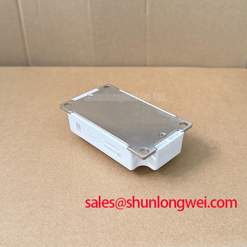
Inspect the module mounting interface, heatsink flatness, fastening pattern, thermal interface coverage, and cooling path before attributing an overload trip to the semiconductor itself. Localized thermal resistance can change both electrical switching behavior and protection response. Uneven mounting pressure, debris between contact surfaces, warped heatsinks, restricted coolant flow, or an unsuitable thermal interface application can produce temperature gradients that are not visible in a static resistance check.
The supplied official specification confirms the Module package classification but does not publish thermal resistance, transient thermal impedance, maximum junction temperature, mounting torque, baseplate dimensions, terminal torque, or cooling requirements. These figures must be obtained from the original module documentation and the equipment assembly data. It is not valid to apply values from a similarly named power module to GT300HF120T2VH.
Design Consideration: evaluate thermal behavior under the actual pulse profile rather than relying only on average power. Transient thermal impedance describes the time dependent path from semiconductor junction to case and then through the thermal interface into the cooling system. Where the relevant manufacturer thermal model is available, engineers can combine the time dependent thermal response with measured or calculated power loss to assess peak junction temperature during repetitive load events. This is an Engineering Calculation only when its loss inputs, thermal model, cooling conditions, and duty cycle are documented.
In a repair investigation, compare the temperature trend of the affected power position with an equivalent known good position under the same controlled load. Thermal imaging can reveal an abnormal external pattern, but it does not directly establish junction temperature. Correlate the image with current waveform, DC bus behavior, cooling conditions, mounting hardware, and the controller fault record. A temperature difference may indicate an assembly issue, unequal load sharing, a cooling restriction, or a drive related loss change that requires further measurement.
Power terminal and gate terminal paths should be reviewed separately. The high current connection should prioritize secure contact and a low loop area. The control connection should prioritize a stable local reference and separation from pulsed load current. Confirm every terminal function from the system documentation before connecting a driver or test instrument, since the supplied official data does not include a terminal map.
For an equipment evaluation involving commercial string inverter or micro grid energy storage hardware, document the measured bus waveform, switching waveform, fault sequence, cooling condition, and assembly condition together. That record supports a technically defensible decision about whether the observed behavior is associated with the module, the gate driver, the DC bus network, the cooling assembly, or the wider control system.