




Content last revised on September 28, 2026
Galvanic Gate Drive Isolation and Transient Verification
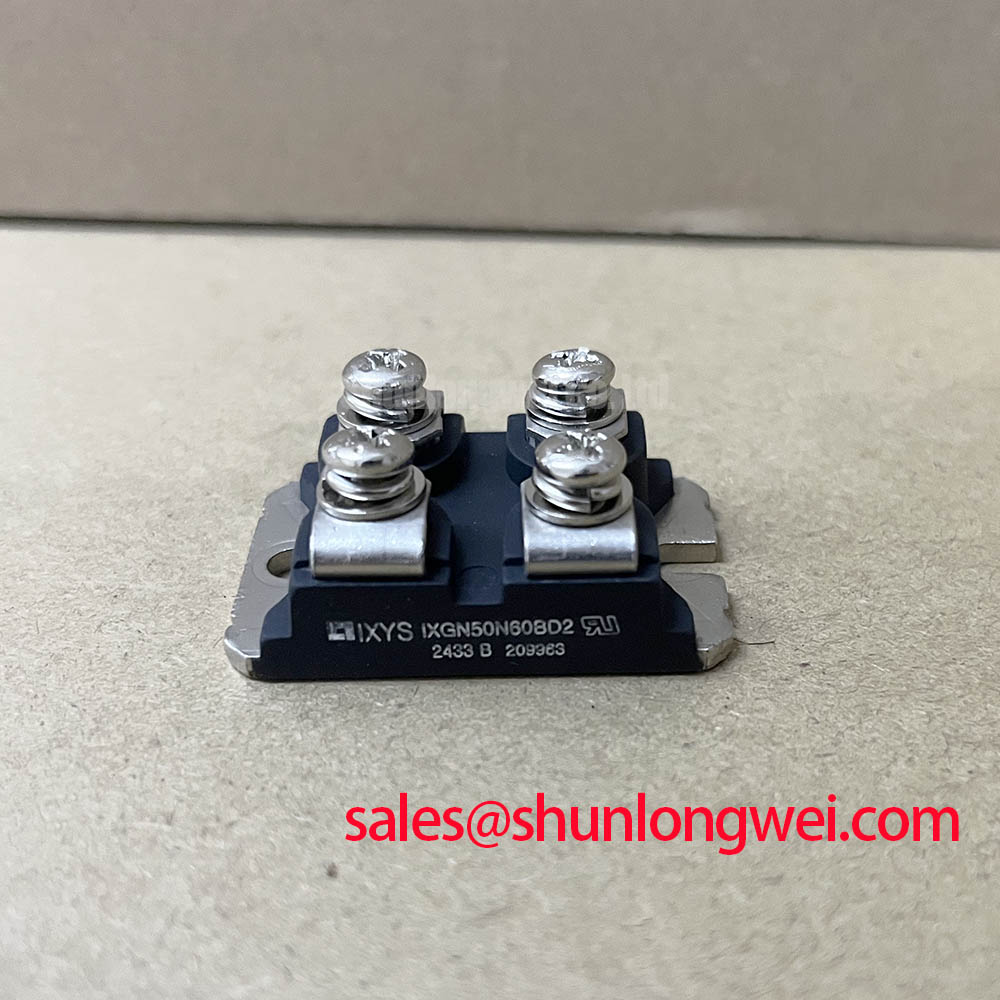
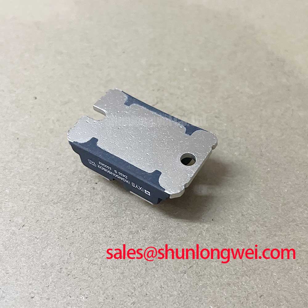
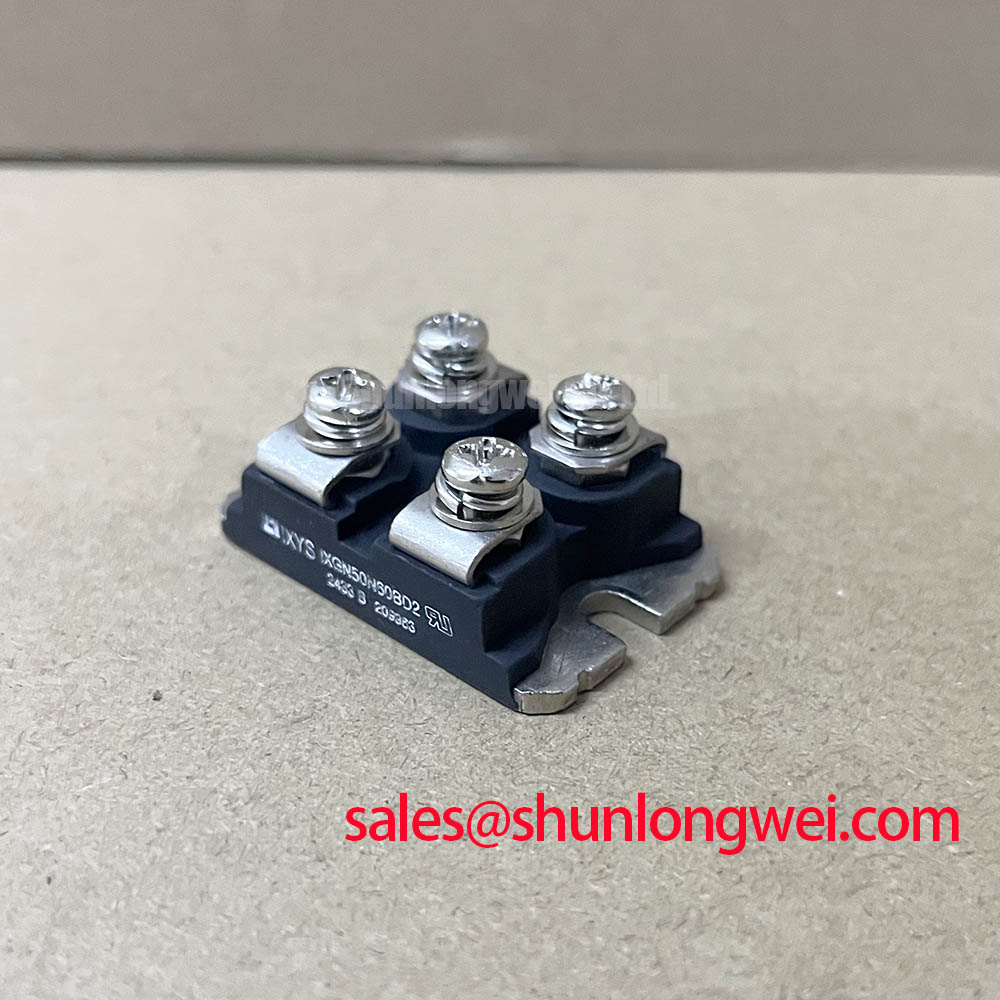
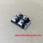
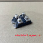
Before fitting IXGN50N60BD2, isolate the inverter, inspect the terminals and package for mechanical damage, and verify the nameplate voltage and current boundary against the replacement record. The device is an IXYS 600 V IGBT intended for evaluation in power conversion equipment such as industrial inverter welders and medium frequency induction heating supplies. Final suitability remains dependent on the switching topology, gate driver, cooling system, and operating waveform.
| Parameter | Value | Engineering significance |
|---|---|---|
| VCES | 600 V | Official Datasheet Specification. Defines the maximum collector emitter blocking voltage. |
| IC110 | 50 A | Official Datasheet Specification. Continuous collector current rating at a case temperature of 110 °C. |
| VCE(sat) | 2.1 V | Official Datasheet Specification. The stated on state voltage used when assessing conduction loss. |
| Eoff | 0.75 mJ | Official Datasheet Specification. Turn off switching energy for the specified test conditions. |
| RthJC | 0.45 K/W | Official Datasheet Specification. Junction to case thermal resistance for thermal path evaluation. |
The first commissioning check should compare the gate driver wiring with the original power stage drawing. Confirm the emitter reference, gate return path, isolation barrier, and driver supply arrangement before applying high voltage. The published device data above identifies the switching element, but it does not by itself certify a reinforced isolation barrier, a specific common mode transient immunity value, or a particular gate driver architecture. Those characteristics belong to the complete driver and isolation system and must be verified from the selected driver documentation.
For a welding inverter or induction heating power supply, minimize the physical loop formed by the driver output, gate connection, emitter return, and local decoupling. This is a Design Consideration rather than an IXGN50N60BD2 factory guarantee. The power circuit and control circuit should maintain the clearance and creepage required by the equipment insulation category, working voltage, pollution level, and applicable safety standard. Designers should confirm those distances from the finished assembly drawing rather than applying a universal spacing value.
During a controlled low voltage test, observe the gate to emitter waveform directly at the device terminals. A clean reference waveform should be compared with the signal measured at the driver output because long probe ground leads can introduce ringing that is not present in the circuit. Check turn on and turn off transitions, the gate plateau, overshoot, undershoot, and the timing relationship between complementary switches. Unexpected pulses may indicate parasitic coupling, inadequate driver return control, isolation capacitance, or measurement error; they should not be attributed to the IGBT alone without checking the complete signal path.
When integrating the device into a half bridge or bidirectional DC to DC battery converter, the system integrator should verify dead time from the actual driver propagation delay, device switching behavior, load current, and temperature. Dead time is a system determined parameter. Excessive dead time can increase diode conduction, while insufficient dead time can create cross conduction. Oscilloscope verification at the gate terminals and collector emitter path is appropriate before the DC link is operated at its intended level.
The external gate resistance should also be selected during bench tuning rather than copied from an unrelated circuit. A larger resistance can reduce ringing and switching stress while increasing transition loss; a smaller resistance can reduce switching time but may increase overshoot and electromagnetic disturbance. The correct value depends on the gate driver source and sink capability, layout inductance, bus voltage, load current, and temperature. The IXGN50N60BD2 data supplied here does not establish a universal external gate resistor value.
Hard Switching Transients, MOV Coordination, and Short Circuit Protection
Inspect the DC link protection network before testing the replacement device. An MOV may help absorb line side or bus transients, but its voltage rating, energy capability, clamping behavior, and ageing characteristics must be coordinated with the DC link and the protected semiconductor. An MOV is not a substitute for short circuit protection, suitable commutation layout, or controlled turn off. The completed network should be validated with a suitably rated differential probe during switching tests.
The listed 600 V VCES rating is an official device boundary, not a recommended operating bus voltage. Switching overshoot is influenced by stray inductance, current change rate, diode recovery, bus capacitor placement, and the mechanical construction of the power loop. Minimize the commutation loop and verify the collector emitter peak against the system voltage margin under the highest credible load and temperature conditions.
Protection timing must be designed around the actual short circuit detection method. The supplied product information does not establish a guaranteed short circuit withstand time, Type I or Type II response, or a universal response below a specified number of microseconds. Those limits require the IXYS electrical specifications and the selected gate driver or protection controller documentation. A protection design can use fast desaturation, current sensing, or another validated method, but the complete chain must be tested for detection delay, gate discharge delay, noise immunity, and fault energy.
A two stage soft turn off sequence is an Engineering Recommendation for evaluation where a hard fault could produce severe inductive stress. The first action should limit gate drive promptly, followed by a controlled discharge profile that prevents an uncontrolled collector emitter voltage rise. The exact timing and gate current are system determined. Engineers should verify the result with fault testing at controlled energy levels and should not assume that a generic soft turn off profile is supported by this particular device.
In the field, a device that fails after a switching event should be examined together with the MOV, snubber, bus capacitor, gate resistor, driver output, and freewheel path. A shorted IGBT does not identify a single root cause. Compare the failed assembly with a known good signal path, inspect solder or terminal joints, and record the bus waveform before replacing multiple components. For a neutral replacement evaluation, engineers may also review the electrical and mechanical compatibility of the CM50DY 28H, subject to the original circuit documentation and system ratings.
Thermal Path, Pulsed Loading, and Benchtop Waveform Tuning
The official RthJC of 0.45 K/W is the starting point for a junction to case thermal calculation. It does not describe the complete path from the case through thermal interface material, heatsink, airflow, enclosure, and ambient environment. When pulsed overload is present, the steady state value alone is insufficient. Designers should use the manufacturer’s transient thermal impedance information, if available, together with the measured pulse duration, duty cycle, case temperature, conduction loss, and switching loss.
The stated VCE(sat) of 2.1 V can be used with the measured collector current to estimate conduction dissipation under the applicable test conditions. The stated Eoff of 0.75 mJ can support a switching loss estimate only when the switching frequency and the original test conditions are comparable. These values should not be treated as fixed across all gate resistance, current, voltage, temperature, or circuit layouts.
For a benchtop evaluation, attach the temperature measurement to the case or heatsink reference point specified by the assembly procedure. Record the case temperature during repeated load pulses and correlate it with the collector emitter and gate waveforms. If the thermal trend changes after cleaning or reassembling the heatsink, inspect the interface material, mounting flatness, contact pressure, and airflow path. A stable electrical waveform does not prove that the thermal path is adequate.
Thermal interface material should be applied as a controlled, uniform layer appropriate to the chosen compound and surface finish. The product information provided here does not specify a universal TIM thickness or mounting torque. Those values should come from the package drawing, heatsink supplier, fastener arrangement, and equipment assembly procedure. Excess material can increase interface resistance, while inadequate coverage can leave air gaps.
⚠️ Maintenance Note: Include heatsink cleaning, fan and duct inspection, contact temperature trending, and terminal torque verification in the preventive maintenance schedule, especially where dust or condensation can alter the thermal path.
At the same time, inspect the equipment for thermal cycling caused by a bidirectional DC to DC battery charger or regenerative power stage. Repeated charge and discharge transitions can produce changing conduction losses and case temperatures. Designers should evaluate the complete thermal cycle rather than infer service life from a single steady load test. No field lifetime or failure rate is established by the parameters listed for IXGN50N60BD2.
For background on switching loss, thermal paths, and selection workflow, the Power Electronics Masterclass provides a broader engineering reference. External package material choices should be confirmed from the relevant manufacturer documents; general information on PPS engineering plastic and silver sintering should not be interpreted as a construction claim for this IXYS device.
Voltage Headroom, Environmental Stress, and Qualification Limits
Verify the actual DC link voltage, line transient profile, switching overshoot, and case temperature before assessing the suitability of a 600 V device. A 230 to 240 V AC input application may be compatible at the system level only after rectifier output, regeneration, tolerance, surge conditions, and switching peaks have been calculated and measured. The device rating alone does not certify a complete inverter or welder design.
Cosmic ray, terrestrial neutron, and single event burnout behavior require application specific reliability data and a defined operating environment. The supplied product parameters do not provide a FIT rate, altitude derating curve, SEB cross section, or guaranteed operating limit above a particular elevation. It would therefore be inappropriate to assign a numerical failure rate or claim a specific altitude capability for IXGN50N60BD2 without an authoritative IXYS source or recognized qualification report.
As a Design Consideration, systems installed at elevated sites should review the semiconductor manufacturer’s high energy particle data, the equipment DC link distribution, enclosure altitude assumptions, and the required voltage headroom. The engineering team should then verify peak collector emitter voltage during normal switching, regenerative events, and abnormal interruption tests. Voltage derating must be determined from documented device data and the complete system risk assessment, not from a generic percentage.
For troubleshooting, capture the collector emitter waveform with an appropriately rated probe while monitoring gate voltage and case temperature. Compare a cold start, warmed operation, minimum load, and maximum intended load. A gradually increasing peak or ringing envelope may indicate a change in commutation inductance, capacitor condition, gate drive behavior, or measurement setup. Confirm the observation with repeatable probing and a known good assembly before assigning a component fault.
Humidity and condensation also deserve attention in workshop and outdoor equipment. Keep the power stage dry during storage and allow temperature equalization before energizing equipment moved between cold and warm environments. Sealing, heater control, conformal protection, and insulation testing are enclosure level decisions. The IXGN50N60BD2 specifications listed above do not constitute an independent EMC, safety, insulation, or environmental certification for the finished machine.