
Content last revised on October 27, 2026
Field Diagnostics & Commissioning: Overvoltage Trip Prevention via Fast-Switching in J2-Q06B-D-W Topologies
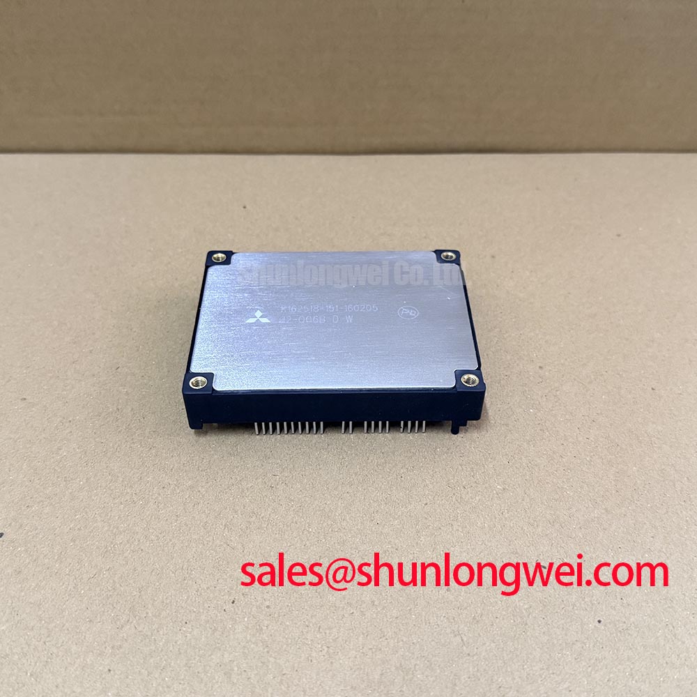
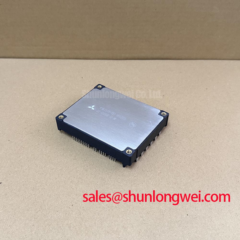
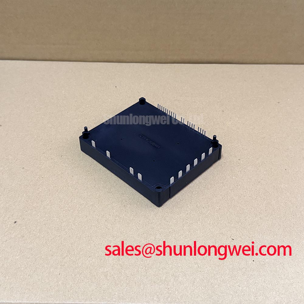
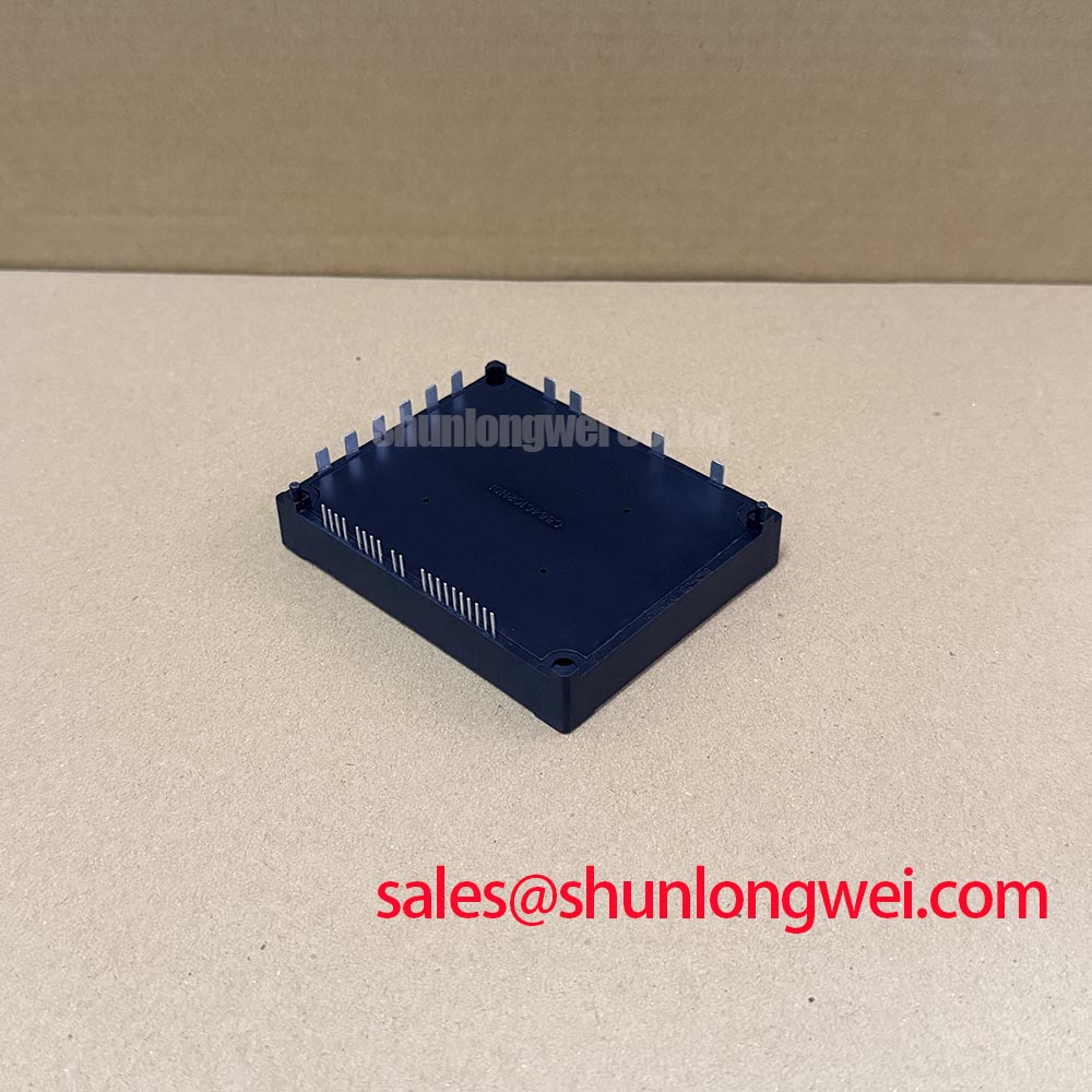
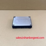
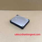
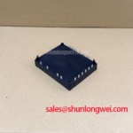
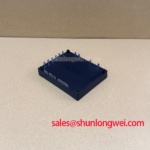
I first correlate a deceleration overvoltage trip with the DC-link waveform and braking command, rather than treating the removed transistor module as the established cause. For J2-Q06B-D-W, the service schematic should establish the switching device’s actual role, its terminal connections and the regenerative energy path. The product classification is a power transistor / Darlington module; it does not establish an internal braking IGBT, integrated gate driver or protection circuit.
Design Consideration: Where the equipment uses a braking chopper, assess its switching device and braking resistor together. Motor deceleration transfers mechanical energy toward the electrical supply; the receiving path must accommodate both the energy of each stop and the repetition of braking events. Resistor pulse capability, average heating, chopper current and the controller’s braking threshold therefore belong in the same assessment. A disconnected resistor, inhibited chopper command or interrupted thermal protection circuit can each contribute to an unsuccessful braking event.
Engineering Recommendation: Compare the braking command with actual current through the resistor branch using appropriately rated instruments. Examine connections after isolation, and preserve the original separation between hot resistor assemblies, control wiring and module terminals. Clearance and creepage requirements depend on equipment working voltage, contamination conditions and applicable insulation requirements; physical proximity alone is not an acceptance criterion.
For potential integration into electric material handling or forklift traction drives, assess regenerative current handling, controller compatibility and the original module mounting arrangement before considering replacement. The 1DI300A-120 provides a separate reference for a structured comparison, not an established equivalent: compare semiconductor type, electrical ratings, terminal mapping, drive requirements and mechanical fit individually.
J2-Q06B-D-W Circuit Protection & Reliability: Calibrating Fault-Clearing Dynamics: Type-I/II Desaturation
Trace the fault signal from the power stage to the drive inhibit before changing protection timing. Design Consideration: Type-I faults describe switching into an existing short circuit, whereas Type-II faults develop during conduction. These conditions impose different current and voltage trajectories. Neither an IGBT short-circuit withstand interval nor a desaturation threshold should be assigned to J2-Q06B-D-W from its model designation or package description.
Engineering Recommendation: Identify whether the installed controller monitors collector voltage, branch current or another fault indicator, then examine its sensing delay, filtering and shutdown path. Desaturation monitoring interprets excessive on-state collector voltage under defined drive conditions; it is not interchangeable with simply checking a static saturation-voltage figure. Fault clearing must fit the selected device’s documented safe operating limits, including the effect of detection delay and current decay.
Design Consideration: A controlled or staged shutdown can reduce inductive voltage overshoot, but extending shutdown also increases semiconductor dissipation. Evaluate that trade-off against the actual transistor technology and driver circuit. For a Darlington implementation, base-drive removal and stored-charge behavior require attention; IGBT gate-resistor settings and negative gate bias are not transferable instructions.
The Evolution of Negative Off-Bias Gate Drive Circuits explains off-state control concepts relevant when evaluating a separate, confirmed gate-controlled power stage. Its guidance does not establish a negative-bias requirement for this module. For manufacturer-level product-family context, consult the Fuji Electric Power Semiconductor & IPM Modules resource while keeping discrete-module characteristics distinct from intelligent-module functions.
Preventing Spurious Faults: Antiparallel Freewheeling Diode Reverse-Recovery Guidelines for J2-Q06B-D-W
Capture the commutation event at the power terminals and the corresponding disturbance at the fault input before attributing intermittent trips to diode recovery. Design Consideration: Establish the freewheeling path from the equipment schematic, including whether the diode is external or documented within the module assembly. Reverse recovery involves the removal of stored charge; an abrupt current collapse can excite circuit inductance and produce ringing that couples into nearby control wiring.
Engineering Recommendation: Evaluate peak reverse-recovery current alongside its decay behavior, switching current, temperature and measurement conditions. A peak value alone does not describe how strongly the surrounding circuit will ring. Keep probe connections compact and use suitable differential measurement techniques so that probe-loop pickup is not mistaken for a device transient. Compare the power-stage disturbance with the sensing circuit’s response to distinguish electrical stress from noise-induced fault reporting.
Design Consideration: An RC snubber can damp an identified oscillation, but its resistance, capacitance, pulse loading and dissipation depend on the measured circuit. Adjusting turn-on gate resistance is relevant only to a confirmed gate-controlled switch elsewhere in the topology; a Darlington stage instead requires assessment of its base-drive network and switching behavior. Neither adjustment should be presented as a universal setting for J2-Q06B-D-W.
Engineering Recommendation: Restore disturbed cable routing and shielding connections before changing suppression components. Keep sensitive signal returns out of high-current commutation paths, and inspect contamination near terminal barriers where moisture can aggravate leakage. Maintenance Note: Trend terminal temperature rise and inspect cooling airflow during planned service, using the equipment manufacturer’s fastening and thermal-interface procedures.
J2-Q06B-D-W Circuit Protection & Reliability: Calibrating High-Frequency Commutation Loop Inductance
Locate the complete high-frequency current loop before moving a snubber or reshaping a bus connection. Design Consideration: The relevant loop includes the switching path, its return and the local energy-storage connection; shortening one visible conductor does not necessarily reduce the whole loop’s inductance. Closely coupled outgoing and return conductors can reduce enclosed loop area, subject to the assembly’s insulation and mechanical constraints.
Engineering Calculation: A first-order estimate expresses switching peak voltage as the DC-link voltage plus the product of stray inductance and current slew rate. This relationship explains why a faster current transition can increase overshoot without any change in the steady bus voltage. It is not a complete prediction of ringing or clamp behavior, so use measured terminal waveforms to assess the actual peak against the device’s documented limits.
Engineering Recommendation: Position suppression components to intercept the relevant transient current without adding a long connection loop. Select snubber capacitance from the required transient response and component pulse capability, then evaluate resistor heating and switching losses under the equipment’s operating conditions. Preserve terminal barriers, specified mounting geometry and service access when assessing planar or overlapping bus conductors. The Fuji Electric Power Semiconductors Portal provides manufacturer product-family information for further component-level comparison.
For maintenance planning, record the restored conductor arrangement and thermal-interface condition so subsequent service does not silently alter the commutation path. Set inspection intervals from the equipment schedule, operating environment and observed thermal trends rather than assigning an unsupported material lifetime. After cold storage or a humid shutdown, inspect for condensation and restore the equipment’s required dry operating condition before electrical testing; finish by checking switching peaks with covers, cooling and wiring returned to their service configuration.