

Content last revised on September 10, 2026
K209A05 Inspection and Repair Evaluation
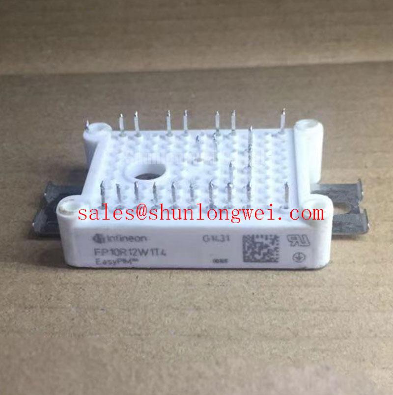
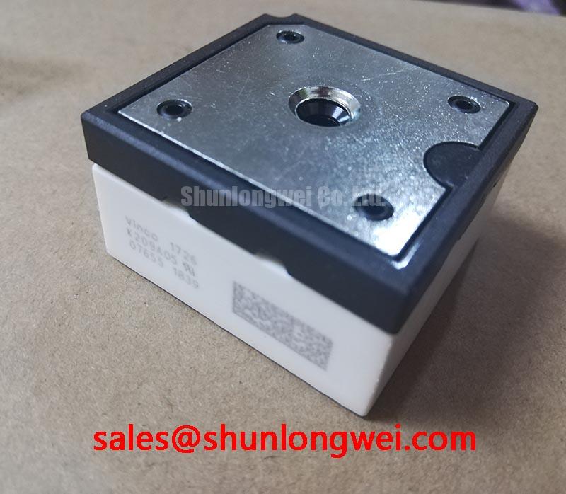
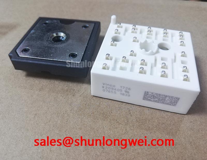
With the equipment isolated and the DC link confirmed discharged, begin by checking the removed K209A05 for cracked housing surfaces, loose terminals, heat spreader contamination, and any visible signs of uneven mounting pressure before comparing terminal connections with the original equipment documentation. This Vincotech power module is officially specified at 1200 V and 8 A, supplied in the flowPIM / flowPACK package family. Those figures identify the electrical rating boundary of the module, but they do not independently confirm the original converter topology, gate drive arrangement, protection threshold, or the terminal allocation used by a particular inverter welder or medium frequency induction heating supply.
For repair evaluation, record the existing module orientation, driver board connector position, busbar stack order, thermal interface condition, and all terminal labels before removal. Cold resistance checks can help identify an obvious short circuit between power terminals, but a multimeter reading alone cannot establish switching health. Gate drive traces, desaturation protection circuits, current sensing paths, snubber networks, and DC link capacitor condition should be checked against the known system schematic or an undamaged matching channel.
| Item | Declared Information | Classification |
|---|---|---|
| Product model | K209A05 | Official product identification |
| Manufacturer | Vincotech | Official manufacturer identification |
| Voltage rating | 1200 V | Official specification |
| Current rating | 8 A | Official specification |
| Package family | flowPIM / flowPACK | Official package information |
Assembly Integrity & Layout Architecture: Implementing Negative Gate Bias versus Active Miller Clamp for K209A05
Before connecting a replacement K209A05, inspect the gate driver board at the module interface rather than assuming that a gate related fault is inside the power module. Fast voltage movement at a switching node can couple through device capacitances and wiring inductance into an inactive gate loop. In a bridge leg, this effect can create unwanted gate movement and may contribute to cross conduction if the driver return path, gate loop routing, or clamp function is compromised.
Negative gate bias and an active Miller clamp are two different control approaches that may be used in power converter gate drive designs. Whether either approach exists in the original equipment must be verified from the driver schematic, measured waveforms, and original service documentation. The official 1200 V and 8 A ratings of K209A05 do not establish a permitted gate voltage range, a required negative bias level, or an active clamp threshold. Those values are system dependent and must not be inferred from the module’s voltage and current ratings.
As a Design Consideration, keep the outgoing gate conductor and its intended return path physically close, avoid sharing that return path with pulsed power current, and inspect connector pins for fretting, looseness, or heat discoloration. A long driver return path can add inductive voltage during switching and distort the voltage that the driver actually applies at the module terminals. Where an active clamp circuit is present, inspect the clamp transistor, its control trace, and associated driver supply integrity before condemning the module.
On a bench with suitable isolated measurement equipment, compare the suspect channel with a known operational channel. Observe gate to emitter voltage at the module connection points, the switching node waveform, and the driver supply response during a controlled operating condition. Ringing, unexpected gate movement, or irregular turn off behavior may indicate a layout, driver, grounding, or protection interaction; each possibility needs evidence from the complete circuit.
⚠️ Field Alert: Tighten power connections in the equipment manufacturer’s specified sequence and use a uniformly thin thermal interface layer, because uneven clamping can impair thermal contact or stress the module package.
For service teams evaluating a different Vincotech device, K420A4001 should be compared only through its verified documentation, including terminal map, switching topology, driver requirements, mechanical fit, and thermal interface details. A shared manufacturer name or voltage class is not proof of direct interchangeability.
Preventing Spurious Faults: Overvoltage Trip Prevention via Fast Switching Guidelines for K209A05
When an inverter welder or induction heating source reports intermittent DC link overvoltage, determine first whether the reported condition is measured at the DC link, detected by a driver protection circuit, or inferred by the controller from another signal. A fault record can be influenced by regenerative energy, capacitor degradation, brake circuit behavior where fitted, sensor reference problems, switching overshoot, or incorrect controller calibration. The K209A05 rating alone cannot identify the cause of a trip.
Some motor drive systems use an external braking transistor and resistor arrangement to dissipate kinetic energy returned to the DC link during deceleration. That architecture should not be presumed for a K209A05 installation or for a welding or induction heating power source. If the original system includes a braking path, engineers should inspect the relevant transistor, resistor assembly, controller command signal, fuse path, and thermal connections using the original circuit information. The power rating of a braking resistor and the switching rating of any braking transistor must be selected from measured energy conditions and the complete system design, not from the module’s 8 A current label.
Fast switching can also produce local voltage excursions where busbar inductance, capacitor placement, and current commutation interact. This is a Design Consideration rather than an official K209A05 guarantee. The practical objective is to minimize the high current loop area between the DC link capacitor, module power terminals, and commutation path, then verify peak voltages during switching tests against the applicable DC link operating condition. A stacked busbar arrangement can reduce loop inductance when it is correctly designed, but its suitability depends on the equipment’s insulation, spacing, current path, and mechanical assembly.
Inspect the DC link capacitors for secure connections and measure them with appropriate test methods. Also inspect snubber capacitors, suppression components, gate driver supply decoupling, and control ground attachments. A poor connection in any of these locations may create waveform changes that resemble a module fault. The background principles of switching conversion and energy transfer are described in Switched Mode Power Supply Topologies and Conversion; equipment level implementation still requires direct testing.
Thermal contact is equally important during replacement work. As an Engineering Recommendation, apply thermal interface material evenly across the intended mounting surface and use a cross pattern tightening sequence where the mechanical design calls for multiple fasteners. The installer should follow the equipment maker’s torque specification for the actual screw size, thread condition, heat sink material, and mounting arrangement. Do not transfer a torque value from another package family without verifying the relevant assembly instruction.
A rectifier or front end component can also affect the stress seen by downstream switching circuitry. In systems where the topology and terminal functions have been confirmed, the P950A can be reviewed as a related component reference. It is not presented as a prescribed companion part or automatic substitute for K209A05.
K209A05 Circuit Protection & Reliability: Calibrating Auxiliary Emitter Return Trace Separation
The terminal arrangement of K209A05 must be confirmed from the applicable package drawing and the original assembly documentation before any assumption is made about an auxiliary emitter, driver return, or sensing terminal. The declared flowPIM / flowPACK package information does not by itself confirm the internal circuit configuration or the availability of a dedicated Kelvin emitter connection. During repair, identify every low voltage control terminal by its published terminal designation and trace it back to the driver board.
Where a power module and driver design provide separate power and control returns, their routing must preserve the original design intent. A shared high current return can create a voltage drop that is added to the gate drive reference during turn on or turn off. That interaction can lead to apparent gate waveform instability, false desaturation detection, altered switching timing, or unexplained protection events. It does not establish a single diagnosis, and it should be investigated with waveform measurements and continuity checks.
As a Design Consideration, the gate driver reference should return through the intended low current path while the main emitter or power return carries the converter current through its intended busbar path. Avoid adding repair jumpers that join these paths at arbitrary points. If a PCB trace has lifted, a connector has been replaced, or a busbar has been reworked, compare the physical return route with an undamaged phase or documented layout before reenergizing the equipment.
Protection behavior should also be observed as a sequence. Check whether the controller enables the gate driver, whether the driver supply remains stable, whether a fault line asserts before switching, and whether the event repeats at a consistent point in the operating cycle. This method separates control side faults from power stage symptoms without assigning a failure mechanism prematurely. The applicable semiconductor terminology and device categories can be reviewed through IEC 60747 8 Field Effect Transistors Standard, while the product specific terminal and operating limits must come from the relevant K209A05 documentation.
For applications such as industrial inverter welding or medium frequency induction heating, a service engineer should verify the original driver scheme, commutation path, cooling assembly, and protection response before replacing the module. The correct approach is to preserve the original electrical architecture, then confirm performance under controlled commissioning conditions.
Transient Dynamics & Electrical Design: Long Motor Lead Reflected Wave Voltage on K209A05
Long output cables can behave as transmission paths rather than simple conductors when switching edges are fast relative to cable propagation time. An impedance mismatch between inverter output, cable, and connected load can create reflected voltage behavior at the far end. Under some conditions, terminal peaks can approach a multiple of the applied DC link voltage. This is a system level transient phenomenon, not an official allowable operating statement for K209A05, and it must be measured in the specific equipment.
The stated 1200 V rating establishes an official device rating, but it does not authorize any particular cable length, switching frequency, motor insulation class, output filter specification, or allowable transient peak. In an inverter system with long motor leads, designers should evaluate voltage at the inverter output and load terminals using correctly rated differential measurement equipment. The result should be assessed against the complete insulation coordination, DC link operating range, converter protection settings, and equipment documentation.
Output reactors, dv/dt filters, sine wave filters, shield termination methods, and cable selection can all influence reflected wave behavior. Their suitability is determined by the load, cable construction, switching strategy, output frequency, enclosure arrangement, and acceptable thermal loss. A filter should not be selected solely from the K209A05 current rating. Before modifying a field unit, verify that the proposed change will not disrupt current sensing, control stability, protective shutdown timing, or the intended electromagnetic compatibility behavior of the complete machine.
In induction heating and welding equipment, output cabling and work coil connections also deserve inspection for looseness, corrosion, damaged insulation, incorrect routing, and unintended parallel return paths. A changed work coil, altered cable length, or poorly secured connection may alter resonant behavior and switching stress. For topology context when reviewing resonant appliance and converter concepts, see Resonant Topologies in Home Appliances. The final verification remains a controlled test of the actual power stage, using the original protection architecture and documented operating limits.