Content last revised on July 10, 2026
Hitachi LMG6381QHGE: A Robust Monochrome Display for Industrial HMIs
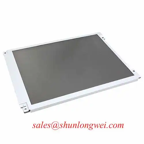
The Hitachi LMG6381QHGE is a monochrome STN-LCD panel engineered for high-clarity data visualization in demanding operational environments. It features a 240x128 pixel resolution, a high-contrast Film STN (FSTN) display mode, and an integrated CCFL backlight. Key benefits include exceptional readability for critical data and a straightforward parallel interface that simplifies system integration. For engineering teams maintaining or designing legacy industrial controls, test equipment, or medical devices, this display provides a proven and reliable solution for non-graphical user interfaces.
Key Parameter Overview
Decoding the Specs for Long-Term System Reliability
The technical specifications of the LMG6381QHGE are tailored for longevity and clear performance in specialized applications. Each parameter is chosen to support integration into industrial and instrumentation systems where readability and reliability are more critical than color or high-speed video.
| Specification | Value & Engineering Interpretation |
|---|---|
| Display Technology | Film Super-Twisted Nematic (FSTN), Monochrome (Black/White) This technology adds a retardation film to the STN structure, which compensates for color dispersion. The result is a highly stable, true black-and-white display, which is critical for reducing eye strain and ensuring immediate recognition of characters and symbols in an industrial setting. |
| Resolution | 240 x 128 Pixels Provides sufficient screen real estate for displaying multiple lines of text, numerical readouts, and simple status icons. This resolution is a well-established standard for compact Human-Machine Interface (HMI) panels, balancing information density with physical footprint. |
| Backlight System | Cold Cathode Fluorescent Lamp (CCFL) Delivers bright and uniform illumination across the display. Unlike modern LEDs, a CCFL system requires an external inverter to supply the necessary high voltage. For an engineer, this means a CCFL inverter must be accounted for in the system's power budget and PCB layout. |
| Signal Interface | 4/8-bit Parallel Data This classic interface is simple to drive with a wide range of microcontrollers (MCUs), even those with limited resources. It eliminates the need for complex signal conversion protocols like LVDS, simplifying both hardware and firmware design, a significant advantage for cost-sensitive or legacy system updates. |
| Operating Temperature | 0°C to 50°C This range defines the ambient temperatures within which the display will operate to its specified performance levels. It is suitable for use in controlled indoor industrial environments, such as factory floors, control rooms, and laboratories. |
Application Scenarios & Value
Achieving System-Level Benefits in Instrumentation and Control
The Hitachi LMG6381QHGE is best suited for applications where unambiguous data presentation is the primary objective. Its design provides direct engineering value in legacy and specialized equipment.
A prime engineering scenario is its use in test and measurement equipment, such as oscilloscopes or network analyzers from a previous generation. In these devices, the critical information is often numerical data, waveforms, and menu options. The FSTN monochrome display of the LMG6381QHGE ensures that this information is presented with maximum contrast and without the color distortion that can occur on lower-quality STN panels. The 240x128 pixel resolution is ample for rendering these elements clearly. The use of a parallel interface simplifies the refurbishment or repair of such equipment, as it interfaces directly with the system's existing digital logic without requiring complex driver board redesigns. This makes the display a practical choice for extending the service life of high-value capital equipment. For applications requiring a different form factor but similar monochrome performance, the LMG6911RPBC offers an alternative set of dimensions and specifications.
Frequently Asked Questions (FAQ)
Getting the Most Out of Your LMG6381QHGE Display
What are the main advantages of an FSTN display like the LMG6381QHGE over a standard STN panel?
The key advantage is superior contrast and the elimination of the typical blue/yellow or gray/green tint found in standard STN displays. The FSTN's compensation film produces a true black-and-white image, making it far easier to read text and simple graphics, which is a critical factor for reducing operator error in industrial control panels.
What is the primary design consideration for the CCFL backlight?
The main consideration is the need for a separate CCFL inverter. This component takes a DC input (typically 5V or 12V) and generates the high AC voltage required to ignite and run the lamp. Engineers must allocate space on the PCB for this inverter and manage its thermal output and high-voltage connections.
Is the LMG6381QHGE a suitable replacement for older monochrome displays?
Yes, its standard resolution and parallel interface make it a strong candidate for replacing end-of-life displays in legacy equipment. However, engineers must verify three key aspects: the physical dimensions, the connector pinout, and the supply voltage requirements to ensure compatibility.
How does the parallel interface simplify integration with an MCU?
A parallel interface connects directly to the MCU's GPIO ports, allowing for straightforward data and command transfers. This is simpler than serial interfaces like I2C or SPI for display data, and far less complex than high-speed interfaces like LVDS. This simplicity reduces firmware complexity and frees up the MCU's dedicated serial peripherals for other tasks.
Why is the contrast ratio specified as 3:1?
The 3:1 contrast ratio is a typical value for this class of transflective STN-LCD technology. While this number seems low compared to modern displays, it was considered effective for high-clarity text-based information in the context of monochrome industrial panels where the distinction between "on" and "off" pixels is clear.
Technical Deep Dive
A Closer Look at the FSTN and CCFL Technologies
The enduring value of the Hitachi LMG6381QHGE lies in two of its core design choices: the FSTN liquid crystal technology and the CCFL backlight. Understanding their engineering implications is key to successful implementation.
The Film Super-Twisted Nematic (FSTN) display is a significant step up from basic STN. Think of standard STN's inherent color shift as trying to see a black-and-white photo through a colored lens. The FSTN display adds a "retardation film" that acts like a color-correcting filter, neutralizing the unwanted wavelengths and producing a crisp, high-contrast black-on-white (or white-on-black) image. This is not merely an aesthetic improvement; for an HMI displaying critical alerts or precise measurements, this level of clarity is a functional requirement for safety and accuracy.
Secondly, the CCFL backlight, while a mature technology, was the industry standard for achieving bright, even lighting before the widespread adoption of LEDs. Its operation is analogous to a standard household fluorescent tube, just miniaturized. The required external CCFL inverter, while adding a component to the bill of materials, decouples the backlight's power system from the display's logic voltage. This can be an advantage in noisy industrial environments, as it isolates the sensitive logic signals from the high-voltage backlight driver circuit, contributing to more robust EMI performance. To learn more about display technologies and their evolution, see this guide to TFT-LCDs.
From an engineer's perspective, the LMG6381QHGE is a component defined by its focused utility. It forgoes modern complexities to deliver exceptional readability and straightforward integration for a specific class of industrial and instrumentation applications. Its combination of a true monochrome FSTN display and a simple parallel interface makes it a durable and practical solution for systems where clarity and reliability are the most important design drivers.