
Content last revised on October 27, 2026
Transient Dynamics & Electrical Design: Baseplate Thermal Grease Layer Control on MEB2066
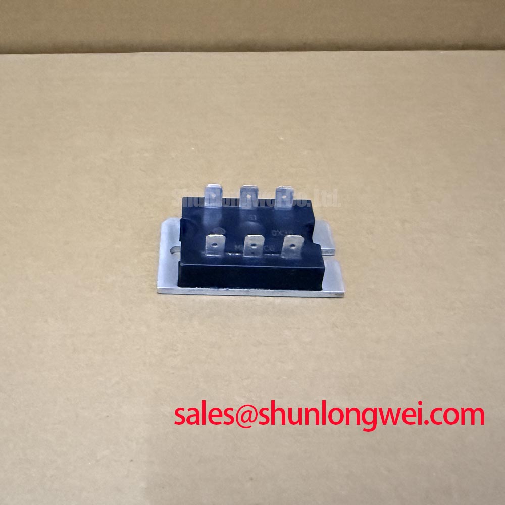
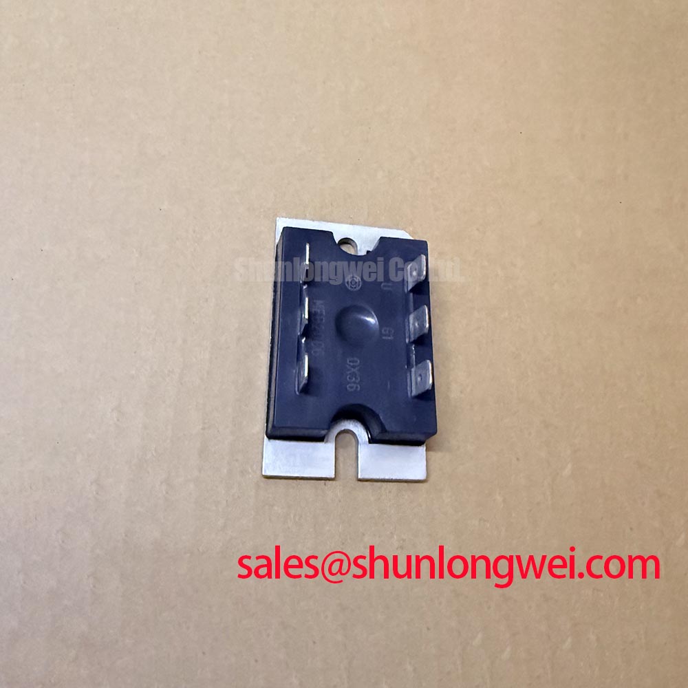
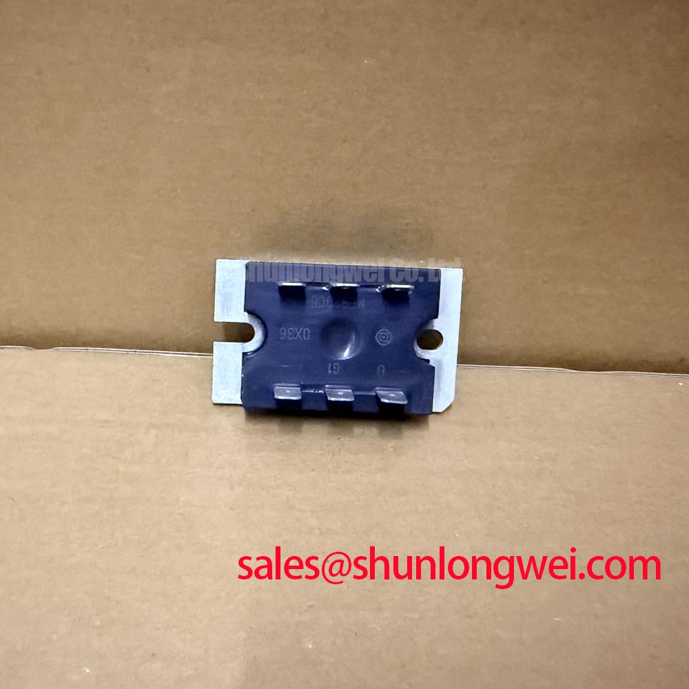
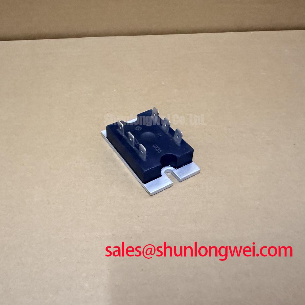
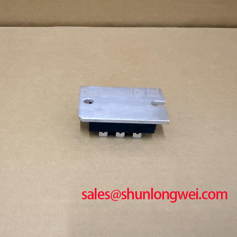
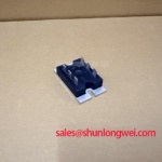
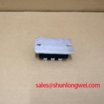
At the service bench, remove the module from the heatsink and inspect the previous thermal interface pattern before installing MEB2066; an uneven imprint often reveals more than a visual check of the enclosure. The published product identity specifies a Module package, a General Power Stage topology, and a Standard series classification from Industrial Manufacturer. No VCES or IC rating is assigned in the available official parameter set, so the replacement review must begin with the original equipment documentation and the electrical limits required by the converter.
For the thermal interface, a controlled compound layer is a Design Consideration, not an MEB2066 factory rating. A practical assembly target may be evaluated in the 50 to 100 µm range when the selected grease, spreader surface, and heatsink flatness support that process. The objective is continuous contact with minimal voiding, not maximum grease volume. Excess compound can increase thermal resistance, migrate toward the terminal region, or make the mechanical stack difficult to control.
Clean both mating surfaces with a process approved for the heatsink and baseplate finish. Do not use a scraper that can score the copper surface. Apply the compound consistently, position the module without sliding it across the heatsink, and bring the fasteners down in a cross pattern. Sequential tightening allows the baseplate to settle while reducing local pressure concentration. The final torque remains a system assembly value determined by the fastener size, thread condition, washer arrangement, heatsink material, and the equipment manufacturer’s mechanical specification.
Thermal compound cannot compensate for a badly distorted heatsink. If the imprint is heavy at one edge and nearly absent at the opposite edge, record the pattern, check the heatsink diagonally, and compare the result with a known serviceable assembly. During electrical validation, monitor case or heatsink temperature together with switching behavior. A temperature rise that appears only under repeated load transitions can be associated with interface quality, current sharing, switching loss, airflow, or control timing, so the investigation should compare several operating states rather than assign a single cause.
Clearance around the module should preserve access for inspection, prevent the thermal compound from reaching conductive surfaces, and keep high current paths short and mechanically stable. Designers should minimize the commutation loop area and verify switching overshoot at the actual DC link, gate drive, and busbar arrangement. The relevant gate resistor, driver output impedance, clamp network, and parasitic inductance are system variables; they are not specified as fixed MEB2066 values.
MEB2066 Operational Boundaries: Evaluating Baseplate Convexity Inspection Limits
Measure baseplate convexity and heatsink flatness before relying on the thermal compound to correct contact. A straightedge, calibrated feeler method, or suitable surface measurement process can identify a high center, a raised corner, or a diagonal twist. The inspection should cover both long and short axes because a visually acceptable edge may conceal a pressure concentration near the mounting holes.
Uniform fastening is a Design Consideration for protecting the substrate and achieving a consistent interface layer. A diagonal cross pattern should be used, with each stage applied progressively rather than bringing one screw immediately to its final value. The 50 to 80 µm interface range described for this integration process is a practical assembly target, not an official electrical or mechanical rating for MEB2066. If the module rocks, the heatsink should be corrected or replaced rather than forced flat by excessive tightening.
For a converter using phase angle control, observe the relationship between commanded conduction interval, line frequency, and thermal response. Uneven conduction can produce localized heating even when the average load appears acceptable. In a commercial string inverter or micro-grid storage system, line-frequency ripple may also pass through the DC link and create recurring thermal movement. Designers should evaluate ripple smoothing within the complete energy storage and control architecture, using measured current and temperature data to establish the actual operating envelope.
RC snubber placement requires the same discipline. A snubber can reduce ringing when its values, voltage rating, pulse capability, and physical location match the switching path, but an incorrectly placed network may add loss without controlling the dominant transient. Inspect the voltage waveform directly at the relevant power terminals with a properly rated differential probe. Compare the waveform before and after the snubber change while recording load, DC-link condition, switching state, and heatsink temperature.
⚠️ Field Alert: Disconnect the DC link and auxiliary supplies before loosening the module or touching its gate and power terminals, then verify the discharge state with an appropriate meter.
For semiconductor switching context, the general principles described in solid-state relay working principles help distinguish a controlled solid-state power path from a mechanical contact path, but they do not define the ratings or internal construction of MEB2066. The module’s actual current, voltage, isolation, and switching limits must remain tied to the applicable device documentation and the converter test plan.
Transient Dynamics & Electrical Design: Four-Quadrant Power Flow Topologies for Grid on MEB2066
Four-quadrant operation changes the thermal pattern because the power stage may alternate between energy delivery and energy absorption. In a battery rack to inverter link, positive and negative active power can occur during charging, discharge, regeneration, or peak shaving. The MEB2066 listing identifies a general power stage module, but it does not assign a specific bidirectional topology, voltage class, current class, or control method. System engineers should therefore map the required switching positions and confirm that the selected power stage is electrically compatible before replacement.
In a four-quadrant arrangement, inspect the DC busbar geometry, return path, gate-drive reference, and current sensor location as one system. Symmetrical paths help reduce unequal commutation stress between parallel or complementary branches. The gate loop should be separated from high di/dt power conductors where practical, while the driver reference should return to the intended emitter or source reference defined by the actual circuit. Avoid allowing control ground currents to share a long path with the power return.
Heavy C-rate peak shaving can create cyclic thermal swings even when the average power over a long interval is moderate. The correct evaluation uses the real dispatch profile, not only a steady resistive load. Record junction temperature indirectly through validated thermal measurements, heatsink temperature, phase current, DC-link voltage, and switching transitions. The resulting thermal profile can then be compared with the package and system limits specified for the final approved device.
Regenerative braking or energy absorption may also require a braking chopper and a high-power braking resistor elsewhere in the topology. That resistor is a system-level energy management element, not an identified feature of MEB2066. Its pulse energy, cooling, switching coordination, and fault isolation should be assessed independently. Where the power stage operates near a control transition, verify that dead time, current direction sensing, and gate-drive interlocks prevent unintended cross conduction.
Long-duration evaluation should include the thermal cycling principles discussed in power cycling and thermal fatigue in semiconductors. This reference explains the general relationship between repeated heating and semiconductor assembly stress; it does not provide field-life figures for MEB2066. For an engineering review, the useful evidence is the measured temperature swing, dwell time, load profile, and inspection result from the actual converter design. The broader integration principles are also covered in IGBT Design & Integration.
MEB2066 Operational Boundaries: Evaluating Driver Power Stage Start-Up Inrush Mitigation Limits
Auxiliary driver power sequencing should be established before the high-voltage DC link is applied. The driver supply must reach its valid operating state, the UVLO interlock must report a stable condition, and the controller must hold the switching commands inactive during the transition. The suggested negative turn-off bias range of −5 V to −15 V belongs to a possible system driver architecture, not an official MEB2066 parameter. The actual gate-emitter limits, driver topology, and required bias must be taken from the approved device and circuit documentation.
Use an oscilloscope to observe the driver supply rails, gate command, gate-emitter voltage, and power-stage response during start-up. The useful sequence is supply enable, UVLO release, controller initialization, gate output authorization, and DC-link connection. If the gate signal moves before the driver supply is stable, investigate the driver enable logic, isolated power start-up, pull-down network, and common-mode transient response rather than changing the module immediately.
Negative turn-off bias can support immunity against Miller-induced gate movement when the driver, insulation system, and device gate limits are compatible. It can also increase stress if the gate-emitter voltage is exceeded or if the return path develops inductive ground bounce. Keep the gate-drive loop compact, route the turn-on and turn-off paths deliberately, and separate the driver reference from noisy auxiliary returns. The system engineer should verify the maximum transient gate voltage at the module terminals during both normal switching and fault interruption.
Inrush control for the driver supply and DC link should be treated as two related but separate functions. Auxiliary supply inrush may disturb UVLO stability, while DC-link charging can stress the precharge circuit, contactor, or input protection network. Confirm that the precharge state is complete before enabling high-energy switching. If a start-up fault is intermittent, capture the timing of the UVLO signal and gate command against the DC-link ramp; this often distinguishes a sequencing disturbance from a power-stage transient.
Common-mode ground bounce deserves attention when the converter uses long connections between the control board, isolated driver, and power module. Use the intended isolation barrier, minimize parasitic coupling from the switching node, and validate the shield termination strategy within the complete enclosure. Cable routing, auxiliary transformer construction, probe placement, and chassis bonding can all affect the observed waveform. MEB2066 is identified only as an Industrial Manufacturer Power Semiconductor in a Module package, so these integration decisions remain dependent on the completed hardware design and its validated operating limits.