



Content last revised on October 29, 2026
MFC130A1200V Identification and Pre-Service Checks
- Isolate the equipment, verify stored energy has discharged, and identify every connected power and control terminal before measuring cold resistance.
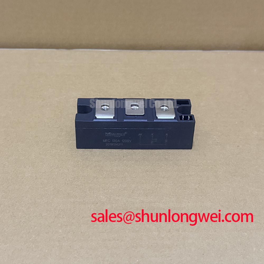
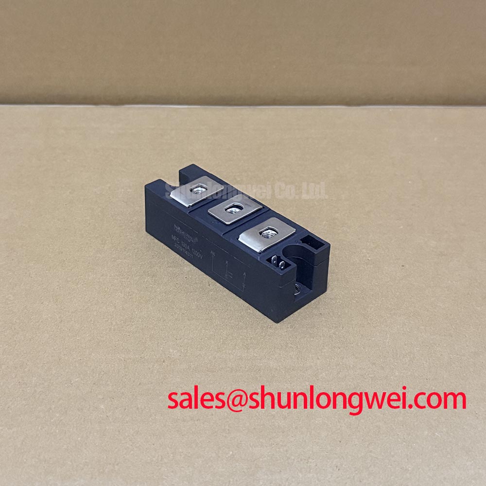
- Record the MFC130A1200V marking, terminal arrangement, and installed orientation against the equipment schematic.
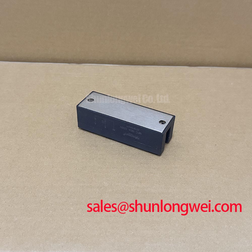
- Inspect the mounting surface, terminal hardware, and thermal interface for uneven contact, contamination, or mechanical strain.
- Disconnect parallel circuit paths where necessary before comparing resistance readings with an equivalent serviceable circuit.
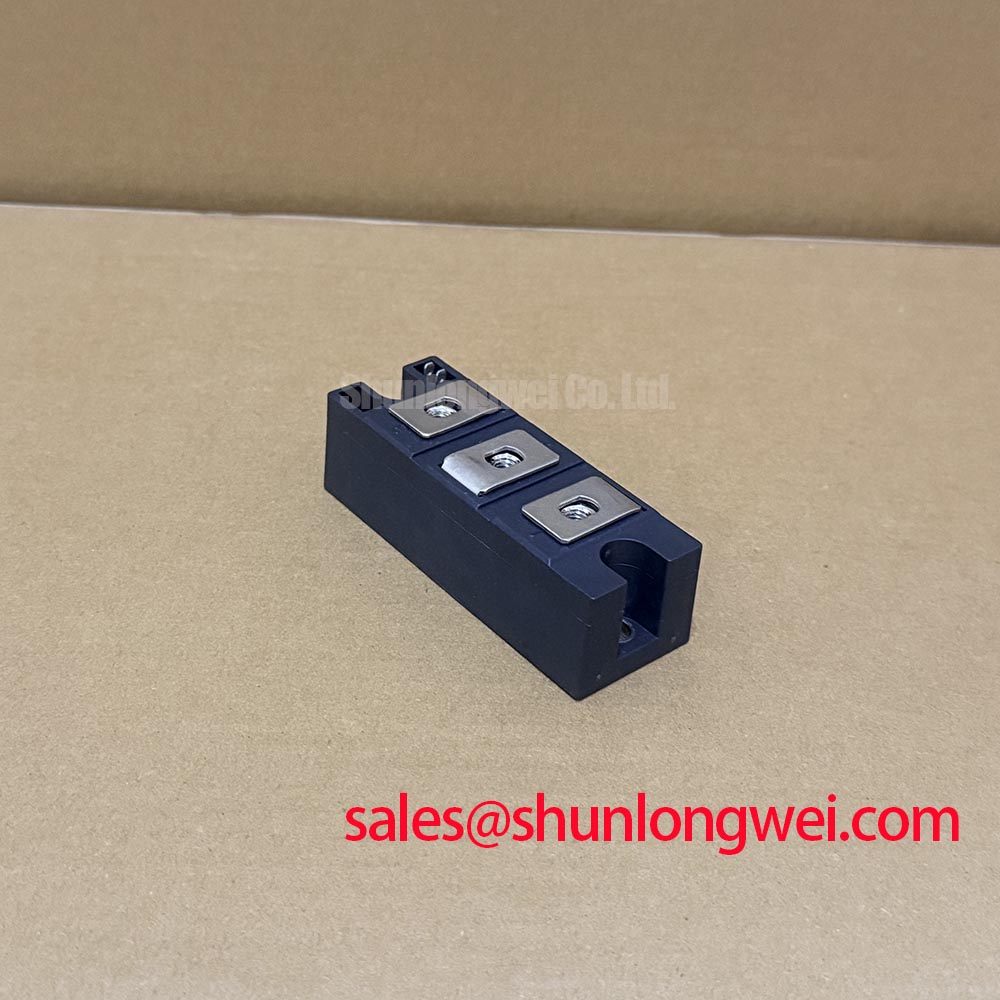
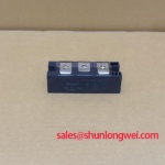
The MFC130A1200V power semiconductor module requires an identity and connection check before a replacement decision. A matching enclosure or similar marking does not establish electrical interchangeability. Keep the original wiring record and mounting arrangement with the service report so that electrical checks and mechanical fit can be assessed together.
| Product identification | Specification or verification status |
|---|---|
| Model | MFC130A1200V |
| Manufacturer | Verify against the module marking and manufacturer documentation. |
| Product category | Power Semiconductor |
| Package | Module |
| Internal topology | Verify against the manufacturer's internal circuit diagram. |
| Series | Verify against manufacturer documentation. |
| Electrical ratings, device technology, and terminal assignment | Consult Datasheet; do not derive ratings or switching behavior from the model string. |
| Dimensions and mounting requirements | Consult the mechanical drawing and installation instructions. |
Field Diagnostics & Commissioning: Turn-Off di/dt-Induced Voltage Peaks and Clamping in MFC130A1200V Circuits
Trace the actual commutation loop before attributing a voltage spike to the module. As a Design Consideration, the relevant loop includes the semiconductor current path, local DC-link connection, and associated return conductor. A long connection or displaced return can increase the voltage developed during rapid current change, even when the replacement occupies the original mounting position.
An Engineering Calculation uses the simplified relationship Vpeak ≈ VDC + Lσ × |di/dt| to estimate the inductive contribution to a turn-off peak. This approximation does not include every resonant or recovery effect. Use it to interpret measured behavior, not to assign a blocking rating to MFC130A1200V or establish a universal clamp threshold.
For a controlled commissioning test, capture the voltage across the relevant switching path with a suitably rated differential probe and a measurement arrangement that minimizes pickup. Compare the transient with current commutation and clamp activity. A ringing trace can contain both circuit behavior and measurement artifacts; changing the probe arrangement helps distinguish them before modifying hardware.
As an Engineering Recommendation, inspect an existing snubber for damaged connections, capacitor deterioration, and changes from the approved assembly. Capacitor selection depends on transferred energy, repetitive dissipation, pulse-current capability, and the measured circuit response. Closely coupled outgoing and return conductors can reduce loop inductance, but conductor geometry must preserve required clearance and mechanical support. Do not substitute an arbitrary inductance target for switching verification.
When assessing transient headroom, use The Ultimate IGBT Knowledge Base as background for IGBT-based circuits, while retaining the actual device documentation as the acceptance reference. Its gate-control discussion applies only after the installed semiconductor technology has been established.
Thermal Management: Thermal Paste Degradation Prevention on MFC130A1200V
Inspect the heat-sink contact surface and the removed thermal interface before cleaning away evidence of uneven seating. As a Design Consideration, displaced compound, localized dry regions, or an uneven contact imprint can justify checking surface condition and mounting alignment. None of these observations alone establishes the cause of an electrical failure.
Apply the thermal interface material using the approved assembly method, with coverage and thickness controlled by the module and material instructions. Excess compound should not be used to compensate for an unsuitable mounting surface. Check flatness against the mechanical requirements rather than attempting to pull a distorted assembly into position through screw loading.
Field Alert: Never use mounting screws to pull a misaligned busbar or module into position; correct the fit before tightening to the documented assembly requirements.
As an Engineering Recommendation, bring mounting fasteners into engagement progressively using the specified sequence and final torque. Keep terminal tightening separate from base mounting: a supported busbar should meet its terminal without imposing bending load. After assembly, check that washers, cable lugs, and conductor edges have not reduced the required creepage or clearance.
Thermal assessment should follow the complete heat path rather than only the accessible case temperature. The general thermal runaway mechanism in power semiconductors explains how temperature-dependent losses can reinforce heating under unfavorable conditions. It does not establish a product-specific operating limit. Where transient thermal impedance curves are specified, engineers can use the documented pulse conditions and loss waveform to assess junction-temperature excursions; a steady-state heat-sink reading cannot represent every short-duration thermal peak.
MFC130A1200V Operational Boundaries: Evaluating Bi-Directional DC-DC Buck-Boost Conversion Limits
Map each commanded current path before treating the module as part of a bidirectional converter. As a Design Consideration, reverse energy transfer requires a suitable combination of semiconductor paths, control strategy, sensing, and protection. A generic power-module classification does not establish those functions or confirm an internal freewheel path.
When evaluating compatibility with a commercial string inverter or micro-grid energy-storage subsystem, designers should compare the documented internal circuit with the battery-side and DC-link-side schematics. Check terminal polarity, current direction, interruption behavior, and protection coverage in each intended operating mode. Bidirectional energy transfer alone does not prove four-quadrant operation; that description also depends on the permitted voltage and current polarities.
During a direction change, review current-sensor polarity and controller behavior alongside the power-stage waveforms. Unexpected current can involve sensor offset, control saturation, commutation timing, or an unintended conducting path. Compare synchronized measurements rather than assigning the symptom to the module from a single resistance or voltage reading.
As an Engineering Recommendation, evaluate repeated loading transitions as thermal events as well as electrical events. Peak-shaving operation can produce changing semiconductor losses and heat-sink temperatures. Assess these changes using the verified device characteristics, the actual operating sequence, and the cooling response. Avoid converting a battery charging-rate requirement directly into a semiconductor current allowance.
For replacement assessment, record the terminal map, conduction paths, documented blocking behavior, cooling arrangement, and mechanical envelope together. Keep approval conditional on those comparisons rather than on a similar model designation.
Assembly Integrity & Layout Architecture: Balancing Switching Dissipation and di/dt for MFC130A1200V
Identify the control interface before changing any external gate resistor. As a Design Consideration, separate turn-on and turn-off resistance is relevant to an applicable voltage-controlled switching circuit; it is not a universal adjustment for every power module. Gate-drive modifications cannot be justified from the MFC130A1200V designation alone.
Where the documented device is an IGBT, compare driver capability, gate-charge behavior, approved gate-voltage limits, and the existing protection circuit before tuning resistance. Slower switching can reduce some overshoot while increasing switching energy. Faster switching can increase ringing or unwanted coupling. The acceptable balance belongs to the measured system response across its intended operating conditions, not to a fixed resistor recommendation.
As an Engineering Recommendation, inspect the gate-return route for shared power-current impedance and unnecessary loop area. Use an auxiliary emitter connection only when the terminal drawing explicitly identifies it. Negative gate bias likewise requires compatibility with the device and driver limits; it should not be introduced as a generic cure for noise.
A thyristor-controlled circuit requires a different review: triggering depends on documented gate-current and gate-voltage characteristics, while turn-off depends on circuit commutation. Changing an IGBT-style gate resistor does not control thyristor turn-off. For phase-controlled equipment, firing-angle changes also affect the supply-current waveform and must be assessed at equipment level.
After any approved driver adjustment, compare switching waveforms, protection response, and thermal behavior with the established baseline. Retain the tested component values and measurement conditions in the service record so the next maintenance intervention preserves the validated configuration.