

Content last revised on October 27, 2026
Toshiba MG75Q1JS40 Overview and Commissioning Checklist
- Confirm the cold state resistance and isolation condition of the main power terminals before energizing the converter.
- Inspect terminal seating, washer contact, thread engagement, heatsink flatness, and signs of mechanical loading around the package.
- Check the gate driver interlock, auxiliary supply sequence, isolation barrier, and turn off command before applying the DC link.
- Record heatsink airflow, dust accumulation, condensation risk, and terminal temperature during the first controlled load test.
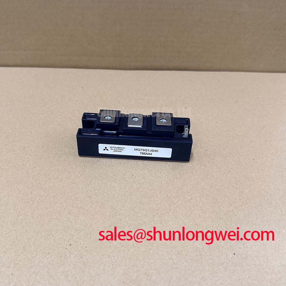
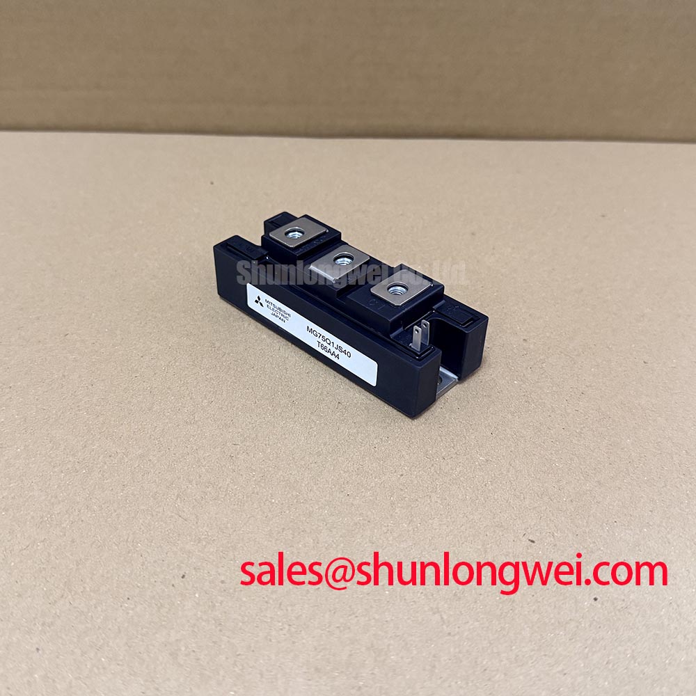
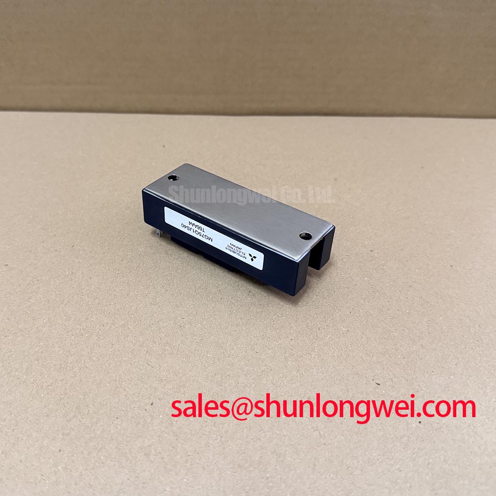
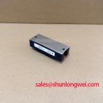
The Toshiba MG75Q1JS40 is an IGBT Module with a specified voltage rating of 1200.0 V and a rated collector current of 75.0 A under the manufacturer's specified conditions. These ratings identify the component class and electrical boundary; the converter designer must still establish switching, thermal, insulation, and protection limits from the complete datasheet and system design.
| Parameter | Value | Classification |
|---|---|---|
| Manufacturer | Toshiba | Product identification |
| Model | MG75Q1JS40 | Product identification |
| Rated voltage | 1200.0 V | Device voltage rating |
| Rated collector current | 75.0 A | Subject to datasheet conditions |
| Package type | Power module | Package classification |
When evaluating this part for a commercial string inverter, battery converter, or microgrid energy storage cabinet, engineers should compare the original switching topology, cooling arrangement, gate drive behavior, and terminal geometry rather than selecting by voltage and current labels alone. Another Toshiba product such as MG150G2DL1 may be reviewed for comparison, but it should not be assumed to be a replacement; electrical and mechanical interchangeability requires a system level assessment.
Field Diagnostics and Commissioning: Preventing Terminal Stress in MG75Q1JS40 Assemblies
Main terminal fastening should be treated as a load path, not only as an electrical connection. Before commissioning, place the module and busbar in their final mechanical positions, then verify that the busbar does not pull the terminal sideways or twist the package when the fastener is tightened. Uneven washer seating, excessive thread engagement, or a busbar that is forced into alignment can transfer mechanical leverage to internal connections. That stress can become more significant as the assembly experiences vibration and repeated heating and cooling.
Use a calibrated tool and the original assembly specification for the terminal hardware. If the original fastening instruction is unavailable, obtain a validated assembly specification rather than copying torque from an unrelated power module or inferring it from screw size alone. Tighten opposing terminals progressively so that the busbar settles without bending. Keep unsupported conductor length short enough to prevent cable weight and vibration from loading the module terminals, while preserving the clearance required by the insulation system.
During a field inspection, look for a terminal that rotates before the nut or screw begins to clamp, a washer that does not sit flat, discoloration around a joint, or a new temperature difference between electrically equivalent paths. These findings do not prove internal cracking, but they justify removing mechanical load and comparing the assembly with a known sound installation. A low resistance reading at rest cannot validate the internal mechanical condition by itself. After correction, use a controlled low energy test and observe terminal temperature, current sharing, and switching behavior under the same operating condition.
The same discipline applies when a replacement is being evaluated. Confirm the mounting footprint, terminal orientation, busbar height, gate interface, and heatsink contact before considering an electrical substitution. The Wide Bandgap Revolution reference is useful when comparing switching technology trends, but it should not be used to assume that a silicon IGBT module and a wide bandgap device share identical drive or layout requirements.
MG75Q1JS40 Thermal Electrical Optimization: DC DC Converter Interleaving and Ripple Current Tuning
In a bidirectional interleaved converter, the converter legs exchange current between the battery rack and inverter link, so thermal inspection must follow the actual power flow in both directions. During peak shaving, a leg that appears acceptable during charging can show a different temperature pattern during discharge. Compare phase current, heatsink temperature, terminal temperature, and switching waveforms at matched operating points. A cyclic temperature rise may involve current imbalance, ripple current, airflow restriction, or thermal interface degradation rather than a single component defect.
The thermal interface material should cover the intended contact area without voids, folds, or contamination. A nominal interface thickness of 50 to 80 μm may be used only as a design consideration when the selected material and surfaces support it; it is not an MG75Q1JS40 factory specification. Surface flatness, clamping pressure, material pump out, and enclosure temperature determine whether that starting point is suitable. Recheck the interface whenever the heatsink has been removed or when measured thermal behavior changes after service.
Mounting screws should be tightened in a cross pattern so the module base settles evenly. The applicable torque is a general mechanical installation consideration determined by the screw, insert, washer, heatsink, and manufacturer assembly instructions. Do not use torque as a substitute for checking contact pressure and flatness. A heatsink with blocked fins or an uneven fan path can produce a temperature gradient that appears electrically as poor current sharing.
For parallel or interleaved paths, keep the power loop geometry symmetrical and route gate drive returns with the intended reference path. Positive temperature coefficient behavior can support current sharing in some operating regions, but dynamic sharing still depends on gate resistance, propagation delay, stray inductance, device temperature, and controller timing. These variables should be checked with phase current probes and appropriately rated differential measurements. MOVs and other transient absorption networks should be coordinated with the DC link, wiring inductance, fault energy, and switching conditions; their voltage and energy ratings are system design selections, not specifications of this module.
Maintenance Note: Clean the heatsink and verify fan airflow during scheduled service while recording contact temperature under a repeatable load.
MG75Q1JS40 Operational Boundaries: Evaluating Gate Driver Auxiliary Power Sequencing and Electrical Stress Limits
The gate drive system must maintain a safe off state when the high voltage DC link is applied, including during auxiliary supply startup and shutdown. The commissioning sequence should confirm auxiliary supply rise time, undervoltage lockout behavior, enable interlock status, and the actual gate to emitter waveform at the module terminals. If the design uses a negative turn off bias, select it using the module and driver specifications, with margin for gate voltage transients; no suitable bias range is established by the product ratings listed here.
Dead time should prevent simultaneous conduction in complementary switching paths, while the required value is determined by driver delay, device turn off behavior, temperature, load current, and the measured switching waveform. A short local gate loop, controlled return path, and suitable damping network help limit ringing. Buffer or clamp behavior should be checked during both turn on and turn off because a clean gate signal at the driver board may not remain clean at the module terminals.
The isolation barrier must withstand the intended common mode transient environment without disturbing the gate command. Optical isolators and digital isolators should be assessed by their specified common mode transient immunity, propagation delay, supply behavior, and fault response. Verify creepage and clearance around the high voltage terminals, especially where contamination, condensation, or dust can reduce the effective insulation margin. Industrial cabinets should also control moisture entry and allow adequate warm up before high voltage switching begins.
During troubleshooting, capture the auxiliary supply, UVLO output, gate to emitter voltage, and DC link timing on the same time base. A missing pulse, irregular turn off, or unexpected driver reset may result from sequencing, isolation disturbance, protection interaction, or excessive switching noise. The corrective action should follow the measured signal path and the driver manufacturer’s limits rather than assuming that the IGBT module alone caused the event.