

Content last revised on October 7, 2026
P405W Operational Boundaries: Checking Overvoltage Trips During Deceleration
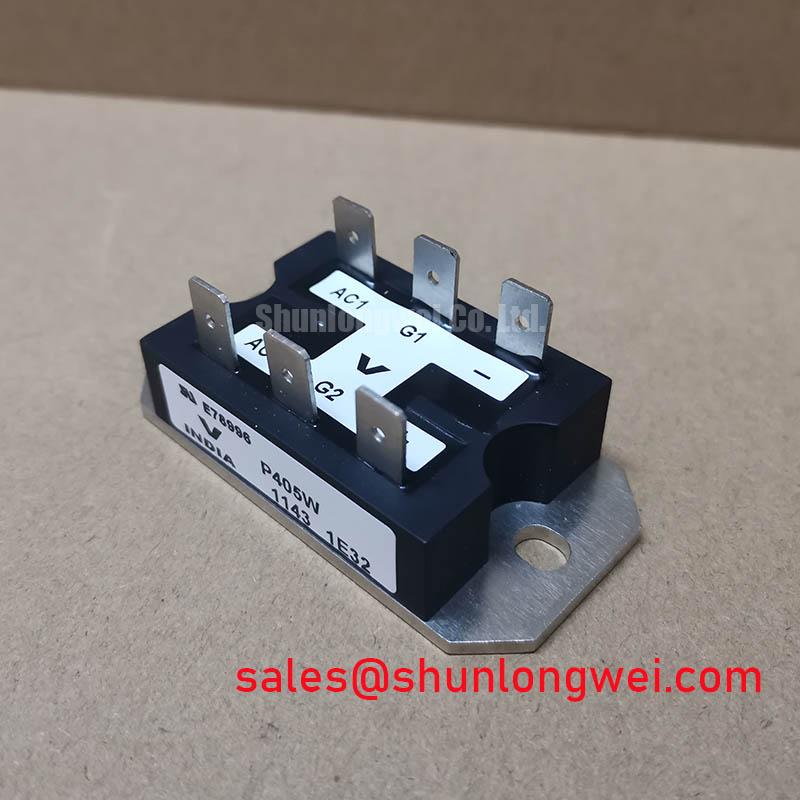
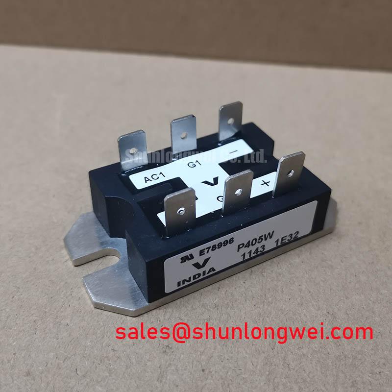
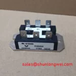
P405W hardware specifications: Manufacturer: Vincotech. Product category: IGBT module. Stated current rating: 2.0 A (Official Specification). Package designation: flowPIM / flowPACK (Official Specification). A numeric voltage rating is not provided in the supplied product specifications.
Capture the DC-link voltage and the drive’s fault indication during a controlled deceleration, then compare the trace with the braking threshold specified for the installed controller. An overvoltage trip can point to insufficient braking capacity, a disconnected braking path, or regeneration exceeding what the system can absorb; the trip alone does not identify a failed P405W.
For a repair assessment, trace the actual braking circuit on the equipment schematic. Confirm whether its switching device is part of the installed power assembly or external to it, and inspect the ballast resistor and its connections without assuming either is contained in P405W. As a Design Consideration, braking-device capability and resistor energy handling must follow the motor’s deceleration duty and the controller’s DC-link limits. Keep switching-loop connections compact to limit inductive overshoot, while determining physical clearance from the complete assembly’s voltage and insulation requirements.
In electric forklift or warehouse-vehicle traction equipment, regenerative braking makes this check relevant, but it does not establish P405W as a compatible traction replacement. If an auxiliary power stage is present, evaluate its schematic independently; SKM100GB063D is a separate device to assess against that stage’s electrical and mechanical requirements, not an assumed companion to P405W.
Benchtop Waveform Tuning: Checking Motor-Lead Voltage Stress
Probe the motor-terminal waveform and the inverter output during a repeatable switching test, using measurement methods appropriate to the installed voltage. A long lead can produce a reflected-wave peak when the cable and motor present a transmission-line mismatch. The often-cited possibility of a peak approaching twice the incident voltage is a Design Consideration, not a P405W voltage rating or a prediction for a particular cable.
Compare terminal peaks, edge behavior, and cable routing before selecting a dv/dt filter or output choke. The filter must be assessed for the drive’s switching behavior, motor insulation, current, and thermal duty; its values belong to the system design. An output choke also brings magnetic forces and mechanical mounting into the assessment. The Maxwell stress tensor describes the underlying electromagnetic force analysis, but it does not provide a mounting specification for this product.
At the power stage, inspect switching-node ringing separately from motor-terminal reflection. Diode reverse recovery, stray inductance, and the commutation layout can all affect that trace. As a Design Consideration, a snubber may reduce ringing, but its losses and effect on switching stress need bench verification. Radiated interference must be evaluated at equipment level; changing a snubber does not establish EMC compliance.
Field Diagnostics & Commissioning: Checking Gate-Drive Return Geometry
Measure the gate waveform against its intended emitter reference while the stage switches under controlled conditions; a gate trace referenced to chassis can hide return-path disturbance. With power isolated and stored energy discharged, inspect gate-drive wiring, connector seating, and the high-current path for looseness or unintended shared return length. Compare cold-state terminal readings with a known-good assembly and the equipment schematic rather than assigning a fault from one resistance reading.
Shared emitter-path impedance can couple load-current changes into a gate-drive measurement. As a Design Consideration, keep the driver return separate from the main current path where the verified module pinout provides a suitable auxiliary emitter connection. The supplied P405W specifications do not establish such a pin; verify the terminal assignment before changing wiring. Compact DC-link and busbar geometry can likewise reduce turn-off overshoot, but the allowable peak must be checked against the actual device rating and measured operating voltage.
For replacement evaluation, compare the mounting pattern, terminal map, current duty, voltage rating, and driver requirements with the installed unit. P546A2005 can be included in that comparison, but its listing alone does not establish a direct replacement for P405W. Field alert: Discharge and verify the DC link before touching gate or power terminals.
Transient Dynamics & Electrical Design: Checking Desaturation Fault Clearing
Record the collector-emitter voltage, gate command, and fault output during a controlled protection test, and establish which signal changes first. A desaturation indication may reflect a genuine overcurrent event or a sensing and timing problem; inspect the sensing path and compare the result with the controller schematic before condemning the module. The distinction between fault conditions present at turn-on and those developing during conduction matters because current buildup and stored energy differ.
As a Design Consideration, fault clearing must be coordinated with the device’s short-circuit safe operating area and the measured turn-off overshoot. A staged soft turn-off can limit the abrupt current change that drives inductive voltage rise, but neither a clearing time nor a two-stage gate profile is specified for P405W in the supplied data. Set those limits only from the verified device documentation and protection-circuit tests. For the switching principles behind those measurements, see The Ultimate IGBT Knowledge Base. In a traction inverter, transformed motor-current measurements may also help distinguish a control event from a power-stage fault; the direct-quadrature-zero transformation explains that control-side representation, not a protection rating for P405W.