

Content last revised on October 5, 2026
P544A0202 Thermal Electrical Optimization: Common Mode Transient Immunity in Harsh Practical Tuning
| Manufacturer | Vincotech |
|---|---|
| Product Model | P544A0202 |
| Product Category | IGBT Module |
| Rated Current | 763.0 A Official Specification |
| Package | flowPIM / flowPACK Official Specification |
Measure the gate emitter path with the power stage isolated, then compare the cold resistance with a known good assembly before applying switching power. A stable reading does not confirm dynamic immunity, so use an oscilloscope to inspect gate voltage during the fastest available switching transitions and look for unwanted pulses that coincide with collector emitter voltage movement.
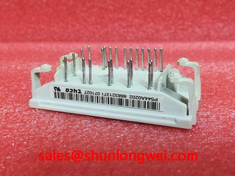
The P544A0202 is a Vincotech IGBT module rated at 763.0 A, with a flowPIM / flowPACK package designation. The supplied hardware data does not establish a numerical isolation rating or common mode transient immunity value. Designers should verify reinforced isolation, gate drive limits, creepage, clearance, and control circuit behavior from the original technical documentation and the complete power assembly.
As a Design Consideration, keep gate drive and power commutation paths physically separated, minimize the shared return impedance, and route the driver reference according to the module terminal arrangement. If a forklift traction inverter shows sporadic gate activity during regenerative braking, capture the driver supply, gate emitter voltage, and switching node on the same time base. Correlation between these traces can indicate coupling or measurement error, but it should not be assigned to one cause without waveform evidence.
For thermal interface assessment, engineers may consult Thermal Diffusivity and Heat Propagation Speed in Substrates when reviewing how mounting surfaces and interface materials affect heat propagation. This is general physics context, not a device specific thermal guarantee.
Transient Dynamics and Electrical Design: Evaluating Thermal Capacitance versus Heat Sink Response
Check the module base, cooler contact, fasteners, and thermal interface after a controlled load test, then compare case temperature rise with the electrical waveform and switching duty. A pulsed overload can produce a delayed case response because junction, baseplate, interface, and heatsink thermal capacitances do not respond at the same speed.
Use the manufacturer’s transient thermal impedance data, if supplied for the exact configuration, to build a multi RC model and calculate junction temperature under the actual pulse profile. Without that device specific curve, do not assign a peak junction temperature margin from a generic graph. The 763.0 A rating remains an official product parameter, not a blanket approval for every pulse width, overload condition, or cooling arrangement.
Minimize parasitic busbar inductance and place high frequency suppression components according to the switching loop identified in the schematic and oscilloscope measurement. Film capacitors or other snubber elements should be selected from measured overshoot, pulse energy, voltage rating, and repetitive stress. The final capacitance and placement are system determined; verify peak voltage against the module’s documented voltage rating during switching tests.
Do not transfer thyristor assumptions such as ITSM, IGT, or VGT to this IGBT module. Those parameters belong to thyristor gate triggering and surge descriptions. For a forklift low voltage traction inverter, verify the actual gate driver current, pulse width, dead time, and protection behavior against the Vincotech documentation for this model.
P544A0202 Circuit Protection and Reliability: Calibrating the Emitter Return
Trace the emitter return from the module terminal to the gate driver reference with power removed, checking for shared copper, loose hardware, damaged lugs, and unintended current paths. If the module drawing provides a separate auxiliary or Kelvin emitter connection, route the driver return independently from the high current emitter path; if it does not, follow the documented terminal topology rather than assuming a Kelvin connection exists.
This separation is a Design Consideration intended to reduce mutual coupling and gate loop disturbance. Confirm the result with differential probing at the module terminals, not only at the driver board. Ringing may arise from layout, probe connection, driver output impedance, commutation speed, or load conditions, so compare the complete signal path before changing gate resistance.
When evaluating MOV coordination, treat the MOV as part of the system protection network rather than as an intrinsic module specification. Select its working voltage, clamping behavior, energy capability, and placement from the measured DC link and transient environment. The module’s official data supplied here does not define a MOV value or surge protection scheme.
⚠️ Field Alert: Disconnect the DC link and allow the specified discharge procedure to complete before touching gate, auxiliary, or power terminals.
P544A0202 Circuit Protection and Reliability: Calibrating DC Link Capacitance Bank Layout and Low ESR
Inspect the DC link capacitor connections first, then measure voltage overshoot at the module terminals with a properly rated differential probe during a controlled switching test. The useful engineering relationship is that peak voltage rises with DC voltage, commutation-loop inductance, and current change rate; the actual clamp limit must be verified from measured waveforms and the module’s documented voltage rating.
Arrange the capacitor bank and busbars to reduce loop area and maintain a symmetrical current path where the mechanical construction permits. Choose low ESR components by ripple current, frequency, temperature, lifetime requirements, and fault coordination rather than by ESR alone. Snubber sizing is an Engineering Calculation based on measured transient energy and repetition rate, not a fixed value that can be assigned from the product name.
For replacement work, compare terminal geometry, package clearance, mounting surfaces, thermal path, and electrical topology before considering another Vincotech unit. The P546A2005 may be reviewed as a separate cross model option, but compatibility remains subject to the original inverter design and documented ratings.
Record the switching waveform before and after installation, including DC link voltage, gate emitter voltage, collector emitter voltage, case temperature, and load current. For broader discussion of industrial drive semiconductor technology and test considerations, see Unlocking Efficiency in Industrial Drives.