
Content last revised on October 23, 2026
Transient Dynamics & Electrical Design: Oscilloscope Waveform Verification on P840A4806
Isolate the drive, verify that its DC link is discharged, and compare the terminal markings on the P840A4806 with the equipment schematic before disconnecting the power stage. Record the existing gate wiring, terminal orientation, and mounting arrangement so that the replacement assessment starts from the actual installation rather than a similar-looking module.
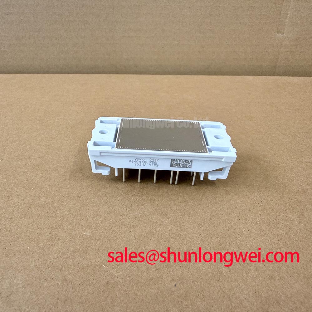
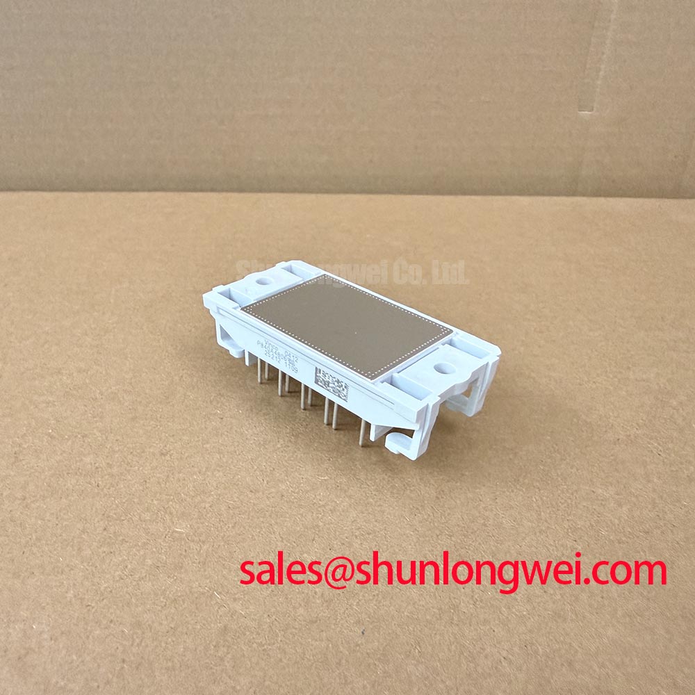
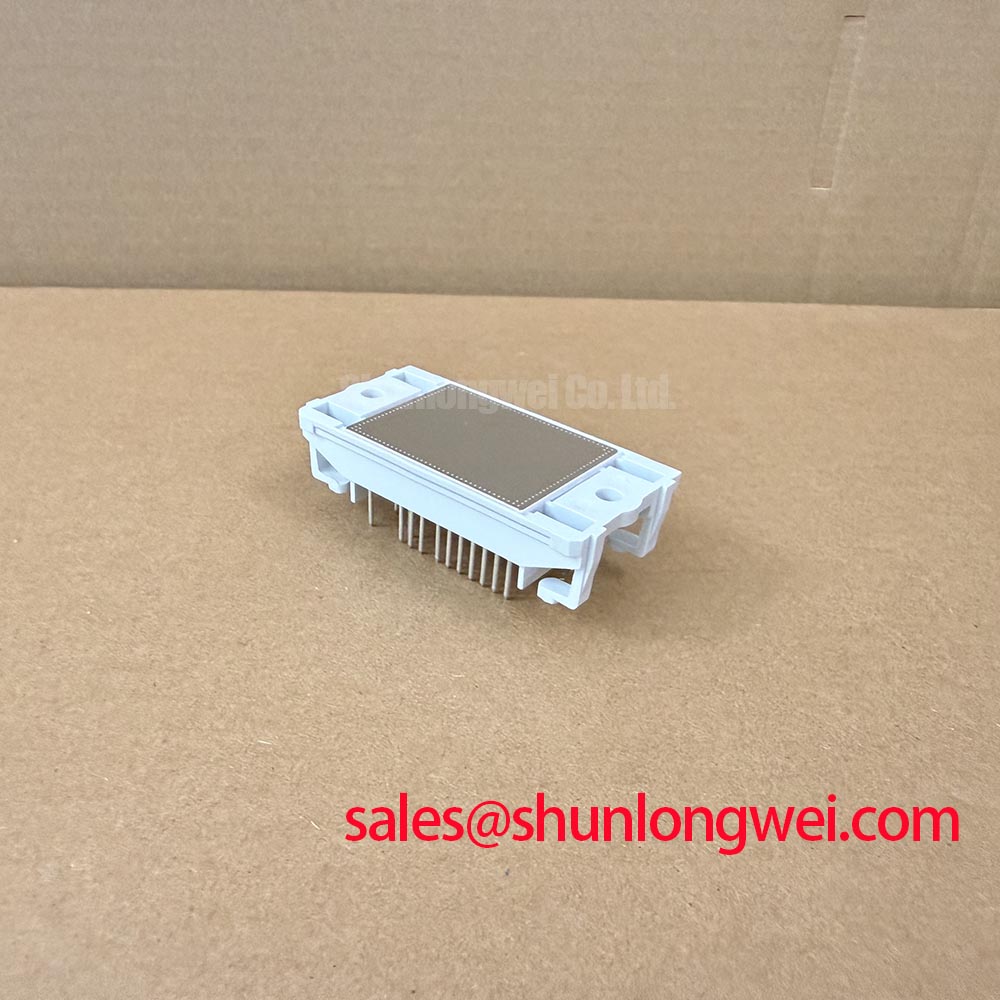
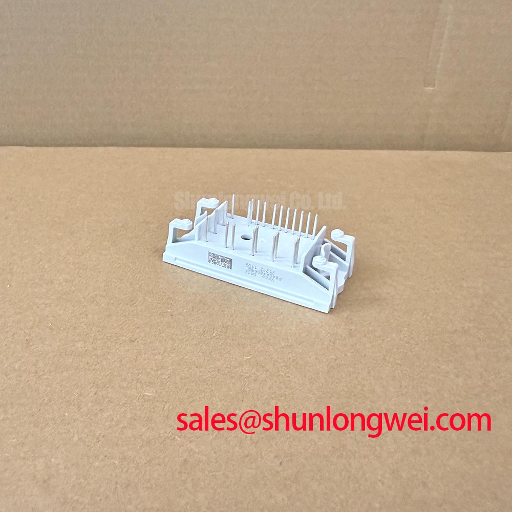
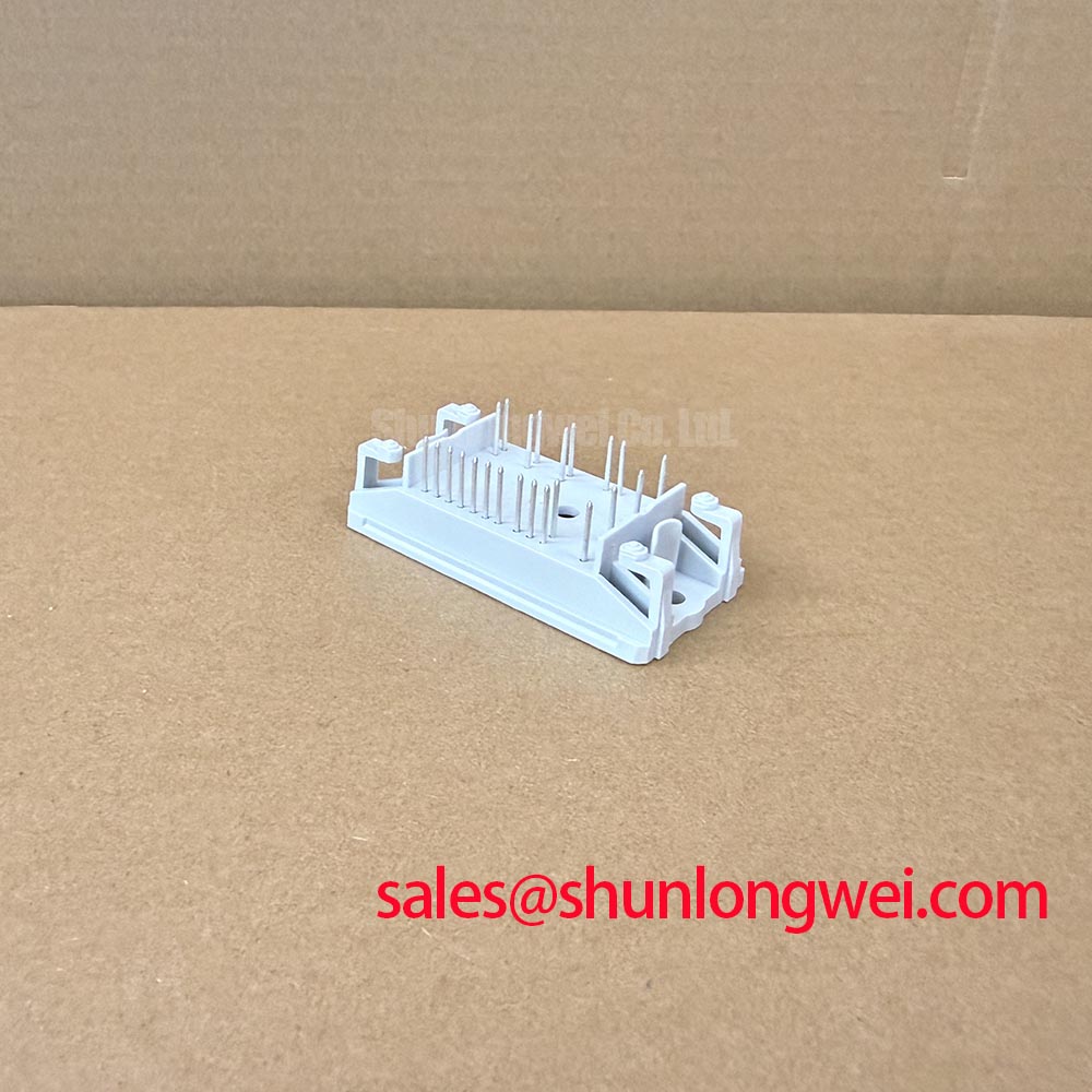
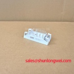
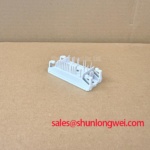
The product identification supplied for this page is Vinco P840A4806, categorized as an IGBT Module with a Module package. The voltage and current entries are “Standard Industrial Rating” and “Standard Operating Current”; these are descriptive labels, not numerical electrical ratings. Obtain the manufacturer’s datasheet for the actual voltage, current, terminal configuration, and operating limits before authorizing an energized installation.
Trace the external turn-on and turn-off gate-resistor paths before changing either resistor on a legacy driver board. As a Design Consideration, establish whether the board provides separate charging and discharging paths, whether steering diodes are intact, and where the driver return joins the power circuit. A resistor change cannot compensate reliably for an incorrect return connection or a damaged driver output stage.
With power isolated, compare the resistor markings and measured resistance against the circuit documentation, accounting for parallel paths that can affect an in-circuit reading. Inspect connector contact pressure, solder joints, and the continuity of the gate connection. A cold measurement can reveal an open path or an unexpected short, but it does not establish switching performance or prove that the module is serviceable under load.
During controlled switching verification, observe gate-to-emitter voltage at the device connection and collector-to-emitter voltage with appropriately rated differential instrumentation. Keep measurement loops compact and follow the probe manufacturer’s connection instructions. Long probe leads can introduce apparent ringing, while an unsuitable reference connection can make the measurement unsafe. Capture the current transition alongside voltage wherever the test arrangement permits.
Gate-resistor adjustment is a system-level tuning task. Increasing resistance can reduce switching speed and associated ringing, while also increasing switching loss; decreasing it can shorten transitions but increase electrical stress. Evaluate turn-on and turn-off independently, changing one variable at a time and retaining waveform records. The acceptable balance depends on the driver capability, module characteristics, operating current, and cooling arrangement, rather than a universal resistor value.
Inspect the commutation loop as carefully as the gate loop. Preserve close coupling between outgoing and return power conductors, avoid unnecessary connection length, and check whether replacement hardware changes the original busbar geometry. These are Design Considerations for limiting inductive overshoot, not verified construction features of P840A4806. The discussion in Mastering Power System Dynamics provides supporting context for evaluating stray inductance and snubber behavior without treating either as a substitute for measured waveforms.
For compatibility assessment in a compact industrial inverter or high-speed CNC spindle drive, compare the complete electrical interface before considering a different module. A comparison with 2MBI100N-060-10 should examine circuit topology, terminal assignment, switching characteristics, gate-drive requirements, and mechanical fit; the linked device is not established here as an interchangeable replacement. Shared product category alone does not demonstrate compatibility.
Assembly Integrity & Layout Architecture: Implementing Fault-Clearing Dynamics with Desaturation Protection for P840A4806
Map the desaturation detection path from the monitored power terminal to the driver fault output, then establish how the controller disables subsequent switching commands. As a Design Consideration, protection review should distinguish a device turning on into an existing short circuit from a short circuit developing during conduction. These fault conditions can produce different current and voltage trajectories, so a single recorded trip event does not validate both.
The protection timing budget includes sensing delay, blanking, filtering, logic propagation, and the actual current turn-off interval. Set that budget against the applicable device short-circuit safe operating area and its stated test conditions. Do not assign P840A4806 a generic short-circuit withstand interval: desaturation detection is a driver function, while allowable fault exposure is a device-specific limit.
Where the installed driver supports two-stage soft turn-off, evaluate how its initial gate-discharge stage limits the current transition and how its final stage holds the device off. A slower fault turn-off can reduce inductive overvoltage but prolong fault-current exposure. Verify the complete response through the equipment manufacturer’s approved test procedure, including fault latching and restart inhibition, rather than introducing an uncontrolled short circuit during field service.
Protection coordination also extends beyond the driver board. The Mersen Protistor® high-speed semiconductor protection fuse range is a relevant manufacturer resource when reviewing semiconductor fuse characteristics. Fuse selection requires coordination with circuit voltage, prospective fault current, clearing behavior, and the protected assembly. A fuse does not replace fast electronic protection, and no particular fuse compatibility is established for this module here.
Restore the thermal interface only after checking the heatsink contact surface for contamination, raised burrs, and damage around mounting locations. Select the interface material and applied quantity using the assembly instructions and its specified application method. Excess material can impede heat transfer, while incomplete coverage can create uneven contact. No universal grease thickness or mounting torque should be imposed on P840A4806 without the applicable mechanical specification.
Field Alert: Tighten mounting hardware progressively in the specified sequence and to the documented torque, rather than using extra force to compensate for poor surface contact.
Where the mounting arrangement calls for a cross-pattern sequence, bring the module into contact evenly before final tightening. Check that busbars and cables meet their terminals without imposing bending loads on the package. Maintain electrical clearance according to the equipment’s insulation design and applicable installation requirements; moving a conductor to improve access must not compromise that separation.
Substrate material should not be inferred from package appearance. The reference on silicon nitride ceramic materials provides general materials background, but does not establish that P840A4806 contains a silicon nitride substrate. For this installation, actionable thermal checks remain contact quality, coolant or airflow condition, and measured temperature behavior under the equipment’s approved operating sequence.
P840A4806 Circuit Protection & Reliability: Checking the Kelvin Emitter Connection
Check the terminal diagram before treating any small terminal as a Kelvin emitter connection. A dedicated auxiliary emitter must be explicitly identified in the device documentation; terminal size or proximity to the gate is insufficient evidence. Where such a connection exists, its purpose is to provide the driver with an emitter reference that avoids the voltage developed across the main current-return path.
As a Design Consideration, route the gate conductor and its intended return together, keeping them away from high-current commutation paths. Shared emitter-path inductance can alter the effective gate-to-emitter voltage during rapid current changes. Separating the driver reference from the power return, where the documented terminal arrangement supports it, can reduce that coupling; it does not eliminate every source of oscillation.
Compare the driver output waveform with the waveform at the module terminals using appropriate differential measurements. Differences can help locate connection inductance, return-path disturbance, or contact problems. Ringing alone does not identify the cause: check its relationship to the current transition and assess whether the measurement arrangement itself changes the observed behavior.
Miller-related gate disturbance requires the same attention to reference placement. Reverse-transfer capacitance and gate charge are different quantities, and neither should be assigned an assumed value for this model. If the driver includes a Miller clamp or active clamping circuit, assess its connection path, activation behavior, and interaction with turn-off using the relevant driver documentation. These are external protection functions, not confirmed integrated features of P840A4806.
After correcting the return path, repeat the approved switching checks across the relevant load conditions and record gate excursions, turn-off overshoot, and temperature behavior. Retain the final resistor configuration, wiring photographs, protection settings, and waveform captures with the service record so that the next intervention can distinguish an intentional configuration from a wiring change.