



Content last revised on September 30, 2026
Field Diagnostics & Commissioning: Long Motor Lead Reflected Wave Voltage in PM75CLS120 Topologies
| Specification | Official Product Data |
|---|---|
| Manufacturer | Mitsubishi Electric |
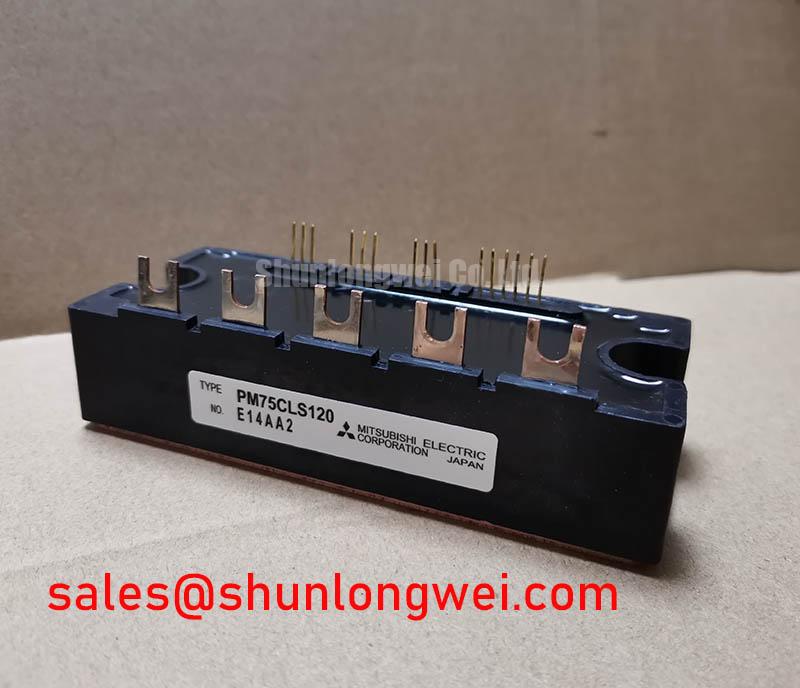
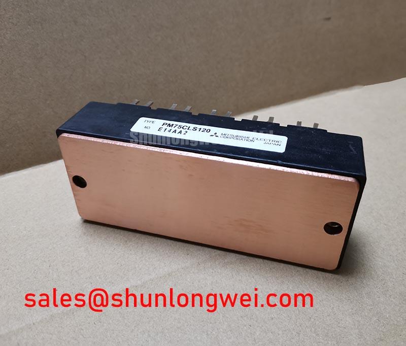
| Part number | PM75CLS120 |
| Product category | IPM intelligent power module |
| Package | Mitsubishi IPM Module |
| Rated voltage | 1200.0 V |
| Rated current | 75.0 A |
Probe the inverter output at the module terminals and at the motor end of the cable, then compare the switching waveforms for reflected voltage, ringing, and abnormal phase imbalance before changing the PM75CLS120. Long motor leads can behave as a transmission line when their impedance differs substantially from the inverter output network, allowing the motor end voltage to rise above the local switching voltage and, in some installations, approach twice the applied DC link voltage at the remote terminal. The observed peak depends on cable construction, length, termination, switching speed, motor input capacitance, and measurement technique, so it must be verified with a properly rated differential probe and a controlled reference waveform.
The PM75CLS120 is specified as a Mitsubishi Electric IPM module with a 1200.0 V rated voltage and 75.0 A rated current. Those ratings identify the device boundary; they do not establish an allowable reflected wave peak for a particular inverter, welder, or induction heating power stage. During commissioning, record the DC link voltage, phase to phase output waveform, phase to ground waveform, gate command timing, and the physical probe connection. A long ground lead on an oscilloscope probe can create ringing that resembles a module overvoltage event.
For an inverter welder or medium frequency induction heating supply, inspect the complete commutation loop rather than only the module. The positive and negative DC bus conductors should follow a compact, low area path to the IPM power terminals, while the output conductors should be routed away from sensitive gate and control wiring. Minimize parasitic loop inductance to reduce turn off overshoot, then verify the resulting peak margin against the DC link voltage during switching tests. The busbar arrangement, capacitor location, cable routing, and enclosure bonding are system design considerations rather than published PM75CLS120 ratings.
When a long motor lead is unavoidable, designers should evaluate an output reactor, dv/dt filter, or sine wave filter according to the motor insulation system, switching frequency, load profile, and thermal limits. The filter must be assessed for its effect on current ripple, control-loop response, leakage current, and fault detection. A filter chosen only from nominal motor power can shift the resonant behavior of the installation and may leave the module exposed to a different transient pattern.
At the bench, isolate the module from the control board and perform cold-state terminal checks against a known-good reference. Verify the polarity of the main terminals and control interface from the applicable Mitsubishi Electric documentation, then use the multimeter diode range only as a comparative screening method. A diode reading is not a substitute for a dynamic switching test, an insulation test, or a complete gate-drive verification.
Bench Diagnostic: Use ESD protection and compare cold diode readings with a known-good reference before connecting the module to an energized DC link.
For manufacturer-level device family information, consult Mitsubishi Electric Power Semiconductors & High-Power Modules. A same-category reference such as PM50B6L1C060 may be useful for a neutral electrical and mechanical comparison, but interchangeability must be confirmed from the original equipment drawings, control signals, protection behavior, and mounting arrangement.
PM75CLS120 Circuit Protection & Reliability: Calibrating Overvoltage Trip Prevention via Fast Switching
Capture the DC link voltage, collector emitter voltage, accessible control signals, and current during acceleration, deceleration, and an intentionally limited fault test to determine whether the protection event begins with load energy, commutation overshoot, control-interface disturbance, or a control timing error. The PM75CLS120 rating of 1200.0 V is an official device specification, while the trip threshold, transient allowance, short circuit withstand behavior, and protection timing require confirmation from the relevant device documentation and the actual control implementation.
During motor deceleration, kinetic energy returns through the power stage and can raise the DC link voltage. The braking path must be evaluated as a system consisting of the braking switch, ballast resistor, DC link capacitor, wiring inductance, thermal environment, duty cycle, and fault controller. Designers should calculate the resistor pulse energy and average dissipation from the equipment load profile, then verify the result through thermal and overvoltage testing. The 75.0 A module rating alone cannot determine the required braking IGBT or resistor size.
A braking IGBT used alongside the PM75CLS120 should be selected by comparing its voltage stress, pulse current, switching loss, short pulse energy, and cooling path with the worst expected regeneration event. The ballast resistor requires attention to pulse overload capability as well as continuous heating. Its connection should keep the high current loop compact and should prevent a resistor fault from bypassing the intended protection sequence.
Desaturation detection and soft turn off are common protection techniques, but values such as a sub 3 microsecond response or a particular two stage timing sequence must not be treated as PM75CLS120 factory specifications without a supporting Mitsubishi Electric source. In practice, protection circuitry should detect an abnormal collector emitter condition, block the normal turn on command, control the turn off behavior, and report the event to the supervisory controller. The complete delay depends on the module’s documented protection behavior, interface timing, wiring, and switching state.
Check the protection waveform with the current probe positioned so that the measurement includes the actual commutation path. An apparent fast protection response can be misleading when the probe misses current flowing through a parallel path. Repeat the test at the intended DC link voltage and temperature range, because switching loss, diode recovery behavior, gate threshold behavior, and capacitor impedance can change the transient profile.
Reverse recovery from the freewheel diode is another source of stress. A diode with a softer recovery characteristic generally reduces the sharpness of the current transition and may reduce radiated EMI, but the actual result depends on junction temperature, commutation current, gate resistance, stray inductance, and the opposing switch. The PM75CLS120 page should not be used to infer an unlisted softness factor or recovery charge. Measure the reverse recovery current and voltage on the real layout when EMI or overshoot is a concern.
Any protective trip should be logged with DC link voltage, load current, switching command state, temperature, and fault timing. This creates a usable correlation between the protection circuit and the operating condition without assigning a single cause from one symptom. Mitsubishi Electric’s broader semiconductor information is available through Mitsubishi Electric Global Semiconductor Device Technologies.
Assembly Integrity & Layout Architecture: Implementing Common Mode Transient Immunity in Harsh Industrial Environments
Measure the control side reference, control signal, and power terminal voltage simultaneously during the fastest switching edge, then inspect whether a control input changes state when the power stage commutates. This test separates a genuine switching command from a common mode displacement that reaches the control interface through parasitic capacitance, connector coupling, shield currents, or an inadequate isolation interface.
The PM75CLS120 is identified by the supplied official data as a Mitsubishi IPM Module rated at 1200.0 V and 75.0 A. The supplied product data does not establish a reinforced isolation withstand value or a common mode transient immunity value for the complete control interface. Claims such as greater than 5 kV isolation or greater than 100 kV per microsecond CMTI therefore belong to the control-interface and isolation design evaluation, not to the confirmed device specification.
Designers should keep high dv/dt power nodes physically separated from logic traces, fault feedback lines, temperature sensing conductors, and communication wiring. Use a clearly defined control reference, avoid routing sensitive traces beside switching copper, and control the return path for displacement current. Clearance and creepage must be selected from the working voltage, pollution environment, material group, altitude, insulation system, and applicable equipment standard. The module package rating alone does not establish compliance with an entire machine insulation standard.
Inspect the mounting interface for contamination, loose hardware, uneven pressure, and unintended conductive paths. The thermal interface should be uniform and free from foreign material, while the busbar should not mechanically load the module terminals. The required fastening method and torque must come from the applicable Mitsubishi Electric mechanical documentation and the equipment assembly standard. Mechanical stress can alter terminal contact quality even when a static diode test appears normal.
When a common mode event is suspected, remove the control command and repeat the waveform capture with the power stage disabled, then compare the isolated control reference against the power switching node. A control signal that remains stable with the power section disabled but shifts during commutation may indicate coupling through the physical layout or isolation barrier. Verify the result using short probe connections and a differential measurement method suitable for the voltage involved.
Wide bandgap switching devices can produce faster voltage transitions than older silicon systems, increasing the importance of isolation layout, gate-loop control, and measurement bandwidth. The related design context is discussed in Wide Bandgap Revolution. That technical background should inform the system review, but it does not add unlisted electrical specifications to the PM75CLS120.
Preventing Spurious Faults: Miller Coupling and Control Interface Guidelines for PM75CLS120
Monitor the inactive switch’s control signal and, where accessible, its gate emitter voltage while the complementary device turns on, because a temporary gate rise can reveal Miller coupling or shared emitter inductance, while a disturbed control signal can indicate coupling at the interface. Cross conduction should be investigated through the complete half bridge timing sequence rather than attributed to the PM75CLS120 from a single waveform.
In designs with accessible gate terminals, an active Miller clamp can hold the inactive gate at a low impedance state during the opposing switch transition. Its usefulness depends on the clamp activation threshold, driver sink capability, gate resistance, common emitter inductance, isolation delay, and the voltage transition produced by the power loop. These are considerations for gate-driver architectures with accessible gate terminals, not confirmed add-on options for the PM75CLS120. The supplied PM75CLS120 data does not confirm an integrated active Miller clamp, a negative gate bias range, or a specified gate voltage for this part.
Negative gate bias is sometimes evaluated where high dv/dt produces unwanted gate movement, but a value such as minus 5 V to minus 15 V must not be applied to this module without confirmation that its gate terminals are accessible and that the bias is permitted. Designers evaluating an accessible-gate design should verify positive and negative gate excursions, driver supply sequencing, turn on and turn off propagation delay, and the effect of the negative bias on fault recovery. A clamp cannot correct excessive common emitter inductance or an unstable isolated power supply by itself.
For designs with accessible gates, keep the gate loop short and separated from the collector or switching node. In the PM75CLS120 installation, keep control-interface wiring separated from high current conductors and follow the documented control-terminal connections. The power loop should also use a low area laminated or closely coupled arrangement where practical, because induced voltage from stray inductance can distort switching measurements.
For incoming inspection, measure accessible terminal and diode paths only as comparative static checks, with the module fully isolated and discharged. Then verify the control connector orientation, terminal polarity, and continuity against the original equipment documentation. A static reading cannot confirm Miller immunity, switching loss, short circuit behavior, or the performance of the protection circuit.
When the module is considered for an industrial inverter welder or medium frequency induction heating supply, validate the entire switching cell under the intended bus voltage, current, temperature, cable arrangement, and protection timing. Confirm that fault feedback reaches the controller without delay that could allow repeated restart attempts. The final decision should be based on measured voltage margins, thermal behavior, control-signal stability, and the documented interface requirements for the specific equipment.