In the semiconductor field, Gallium Nitride (GaN), as a third-generation semiconductor material, is often compared to Silicon Carbide (SiC). Despite not having as long a development history as SiC, GaN continues to showcase its superiority with features such as a large bandgap, high breakdown voltage, high thermal conductivity, high saturation electron drift velocity, and strong radiation resistance.
While GaN may not be as widely adopted as SiC, the attractiveness of GaN is undeniable. According to the GaNPower2021 report released by Yole Developpement, the GaN power market is expected to reach a scale of 1.1 billion USD by 2026.
However, behind this promising development, GaN faces various technical challenges.
1. Substrate Material Issues: The compatibility between the substrate and thin film lattice significantly influences the quality of GaN thin films. The most commonly used substrate currently is sapphire (Al2O3). While it is widely used due to its simplicity, low cost, and good thermal stability for growing large-sized films, the large difference in lattice constants and coefficients of thermal expansion with GaN may result in defects such as cracks. On the other hand, the unresolved issue of single-crystal substrates for heterogeneous epitaxy leads to high defect densities. The large polarity of GaN makes achieving good metal-semiconductor ohmic contacts through high doping challenging, making the manufacturing process more complex.
2. GaN Thin Film Fabrication Issues: Traditional methods for GaN thin film fabrication include Metal-Organic Chemical Vapor Deposition (MOCVD), Molecular Beam Epitaxy (MBE), and Hydride Vapor Phase Epitaxy (HVPE). While MOCVD is suitable for large-scale production with a short growth cycle, the need for post-growth annealing may result in film cracking, affecting product quality. MBE is only applicable for the preparation of a small amount of GaN thin films and is not suitable for large-scale production. HVPE produces high-quality GaN crystals and has a fast growth rate at higher temperatures, but the high-temperature reaction poses challenges in terms of production equipment, costs, and technical requirements.
3. GaN Seed Crystal Acquisition Issue: Directly cultivating a two-inch seed crystal using the ammonia thermal method takes several years. Therefore, obtaining high-quality, large-sized GaN seed crystals remains a challenge.
4. Other Technical Issues: Additionally, GaN currently faces two technical challenges. Firstly, regarding the current growth substrate of silicon carbide, the size limitation has not yet surpassed 6-inch wafers. The high cost of acquiring silicon carbide makes it impossible for large-scale production, keeping prices high. Secondly, the industry needs to overcome the technical challenge of enabling GaN to grow on silicon wafers with high efficiency. If these challenges can be overcome and existing infrastructure utilized, the future prospects for GaN in terms of both price and production volume are expected to improve.
Despite these challenges, where there are difficulties, there are also new technologies.
Undoubtedly, research and development efforts are continuously addressing these challenges, leading to breakthroughs. A collaborative team from China and Switzerland has significantly improved the performance of GaN devices by developing a multi-channel GaN power electronic device technology that approaches theoretical limits.
Crystalwise Semiconductor achieved a breakthrough in 300mm silicon-based GaN High Electron Mobility Transistor (HEMT) epitaxial technology in September 2021. This followed their successful commercial launch of 200mm GaN-on-Si HV HEMT epitaxial wafers in 2014. Vertical breakdown voltage measurements indicate that 300mm wafers are suitable for power device applications at 200V, 650V, and 1200V.

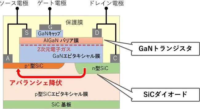
AIST in Japan announced the successful development of the world’s first integrated single-chip prototype featuring GaN HEMT and SiC SBD on December 12, 2022. To address the reliability issues of GaN HEMT, AIST conducted research and development on hybrid transistors, integrating GaN transistors and SiC diodes on the same substrate (i.e., monolithic integration).

Developing hybrid transistors combining GaN and SiC requires establishing an environment for prototyping integrated devices, leading AIST to expand a 4-inch prototype line for SiC power devices, serving as a shared prototype line for both SiC and GaN development.
Despite facing numerous technical challenges, the continuous efforts in research and development are steering GaN toward a promising future in the semiconductor industry.