



Content last revised on October 29, 2026
Preventing Spurious Faults: Active Miller Clamp Implementation Guidelines for SK25GD063
Field failures in precision stepper and BLDC motor servo motion actuators often manifest as catastrophic inverter leg shoot-through during aggressive commutations. In modern bridge legs utilizing the SK25GD063 Semitrans IGBT module by Semikron, high transient collector-emitter displacement currents (Cres × dv/dt) inject charge directly into the inactive gate through parasitic collector-gate Miller capacitance. When the complement switch turns on rapidly, this displaced charge flows through the internal gate resistance, pulling the gate voltage past the threshold level and inducing instantaneous cross-conduction. To eliminate false triggering without introducing excessive switching loss from oversized series resistors, implementing an active Miller clamp network is standard design practice.
The active clamp circuitry senses the gate-emitter potential of the lower or upper switch during turn-off. Once the gate terminal falls below a threshold (typically around 2.0 V to 2.5 V relative to the negative rail), a low-impedance auxiliary clamping transistor shorts the gate directly to the negative bias return pin. This low-resistance shunt bypasses the main turn-off resistor, providing a safe path for parasitic capacitive currents. Applying a dedicated negative gate bias between -5 V and -15 V further widens noise margin against high dv/dt transients, keeping spurious voltage spikes well beneath conduction thresholds. When engineering gate topologies for industrial drives, review foundational mitigation techniques documented in https://www.slw-ele.com/mitigating-parasitic-turn-on-pto-in-sic-mosfets-the-critical-role-of-miller-capacitance-and-threshold-voltage-optimization.html to evaluate how internal Miller capacitance dynamics govern solid-state bridge reliability.
Physical PCB layout rules dictate how well active clamping performs under field stress. The clamp circuit loop—consisting of the auxiliary MOSFET, the gate terminal, and the auxiliary Kelvin emitter terminal—must be routed with minimal loop area directly adjacent to the power module pins. Trace inductance inside this loop must remain negligible to prevent clamping delays. When troubleshooting erratic overcurrent trips or desaturation faults on a downed actuator drive, verify clamping effectiveness with an isolated differential probe directly at the module pins. High ringing amplitudes observed during opposing diode recovery indicate excessive gate trace inductance or an under-damped gate circuit requiring immediate track revision or snubber damping adjustments.
SK25GD063 Operational Boundaries: Evaluating Junction-to-Case Thermal Network Simulation Limits
High-duty cycle motion systems subject power modules to dynamic pulsed thermal overloads during rapid acceleration and emergency braking sequences. Calculating transient junction temperature (Tj) requires analyzing the module transient thermal impedance network, typically modeled using Foster or Cauer multi-RC equivalent circuits derived from physical layer thermal resistances and thermal capacitances. Under intermittent pulsed loads, steady-state thermal resistance calculations fail to predict instantaneous peak silicon temperatures because the heat sink thermal mass cannot respond to microsecond-scale thermal surges generated within the silicon die and copper baseplate.
For system rectifiers or auxiliary charging circuits supporting the main DC bus, selecting robust complementary stages such as the SKKQ800/18E ensures upstream line-frequency ripple smoothing and uncontrolled surge absorption remain well within system thermal thresholds. Thermal modeling across the DC link must also incorporate switching losses (Eon and Eoff), diode reverse recovery losses (Erec), and continuous conduction losses across alternating motor commutation angles. Snubber networks placed across the DC bus mitigate inductive voltage spikes during fast IGBT turn-off by providing an alternate high-frequency return path, absorbing transient energy that would otherwise generate excessive peak dissipation within the semi-insulated housing.
When selecting direct or functional replacements for legacy Semitrans units in motor drives, field technicians must cross-reference mechanical footprint, pinout alignment, and internal barrier parameters. The operational comparison below outlines electrical and mechanical differences across key industrial replacement candidates:
| Parameter / Feature | Semikron SK25GD063 | Semikron SKM195GB066D |
|---|---|---|
| Product Category | IGBT Module | IGBT Module |
| Module Topology | Half-Bridge Dual IGBT | Half-Bridge Dual IGBT |
| Package Platform | Semitrans | SEMITRANS 2 |
| Factory Baseline Status | Standard Legacy Series | Trench / Field-Stop Industrial Standard |
| Direct Replacement Link | Original Equipment Specification | SKM195GB066D (Evaluation Candidate) |
| Mounting Torque Guidance | Design Consideration: Match M5 bolt torque | Design Consideration: Match M5 baseplate specs |
⚠️ Field Alert: When reseating or replacing power modules on service heatsinks, always ensure thermal interface material (TIM) is applied in a clean, uniform layer strictly between 50 to 100 micrometers thick, tightening M5 baseplate mounting bolts progressively to standard industry torque limits (2.5 to 3.5 N·m) to prevent ceramic substrate micro-cracking.
SK25GD063 Thermal-Electrical Optimization: Differential Gate-Source Loop Routing to Solve Oscillation
High-frequency oscillation in switching half-bridges frequently stems from common impedance coupling between the high-current power path and the sensitive gate control loop. In industrial drive hardware incorporating the SK25GD063, high output emitter currents (ie) generate steep di/dt transitions across stray loop inductances. If the driver reference is mistakenly connected to the main power emitter tab instead of the designated auxiliary Kelvin emitter terminal, the induced voltage drop across the parasitic emitter track injects directly into the gate loop. This unwanted negative feedback slows switching speeds or induces sustained high-frequency gate oscillations that trigger rapid thermal destruction.
To establish clean gate signals, power stage PCB routing must implement strict physical decoupling between drive and output loops. The forward gate trace and the auxiliary emitter return path should run as tightly coupled differential pairs, either as stacked traces on adjacent PCB layers or parallel traces closely routed on the same layer to cancel mutual magnetic flux. Keep the loop area between the gate drive isolation transformer, gate resistors, and the IGBT terminals as small as possible. Isolating signal returns and avoiding shared ground copper ensures that high di/dt transients circulating within the inverter motor phases do not cross-couple into low-voltage gate drive circuitry.
Engineers retrofitting or troubleshooting high-power drives should refer directly to Semikron-Danfoss SEMITRANS® Industry Standard IGBTs application benchmarks when verifying mechanical layout tolerances and creepage specifications. When verifying field repairs on high-current servo axes, perform initial commissioning checks under no-load conditions with low bus voltage. Monitor the gate-emitter waveform via a high-bandwidth oscilloscope probe directly across the module control pins. The waveform during turn-on and turn-off should exhibit smooth, monotonic transitions without step distortions, prolonged Miller plateaus, or ringing bursts that exceed standard noise immunity limits.
[-----more-----]
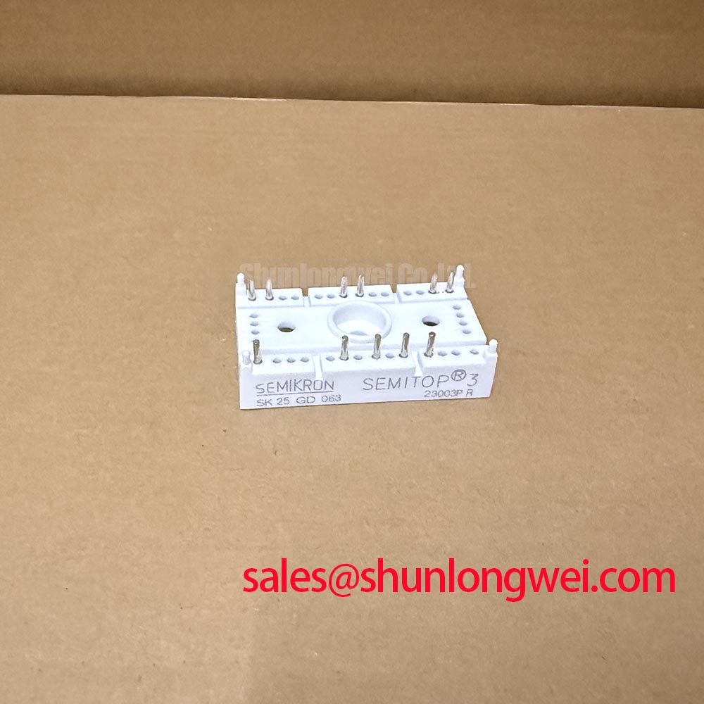
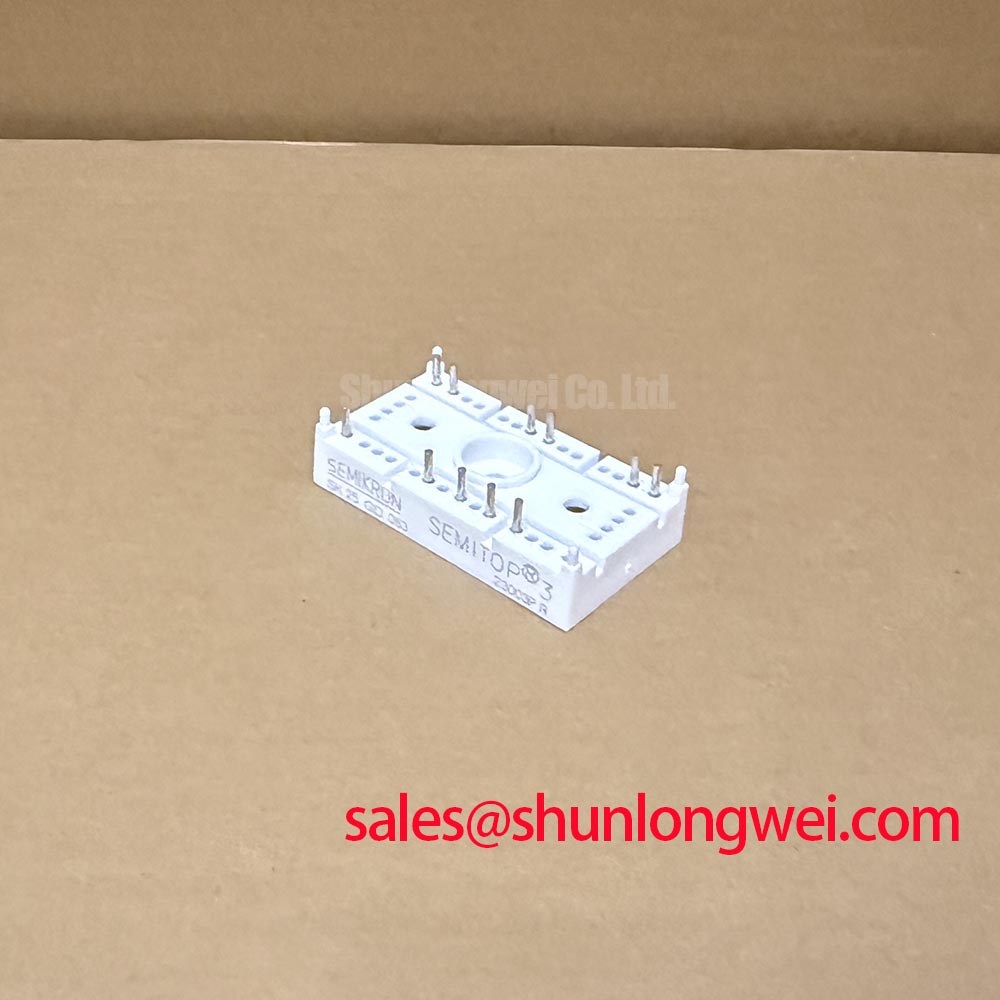
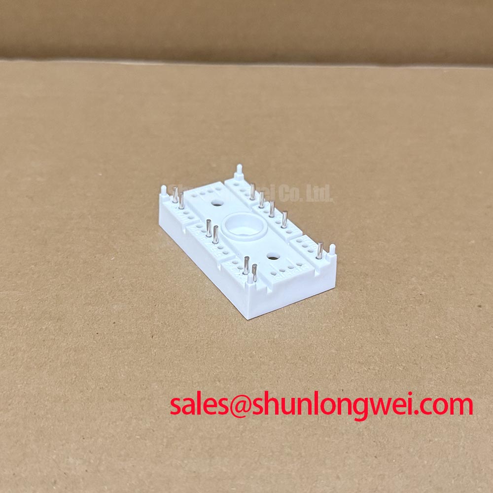
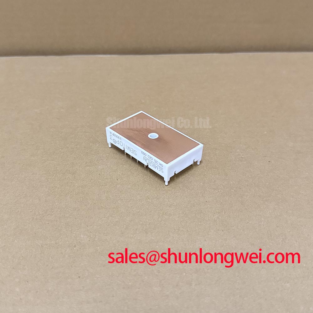
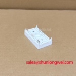
SK25GD063 Semikron Half-Bridge Dual IGBT Module
3
SK25GD063 Semikron IGBT Module | Semitrans Motion Control
Genuine SK25GD063 Semikron replacement unit for Precision Stepper & BLDC Motor Servo Motion Actuator systems. Verified Semitrans module in stock at Shunlongwei.