
Content last revised on September 10, 2026
Preventing Spurious Faults: Dynamic Power Loss Dissipation and Multi-R Guidelines for SKM200GB063D
Begin incoming inspection with the power terminals isolated and the device fully discharged, then verify the marked collector, emitter, gate, and auxiliary connections against the original equipment drawing before applying any test voltage. For a cold-state baseline, use a calibrated multimeter on diode-test mode and record the forward conduction reading of the integrated freewheel diode in the correct polarity. Do not interpret a single meter value as a complete health judgment; compare the result with a known-good reference and inspect the complete commutation path.
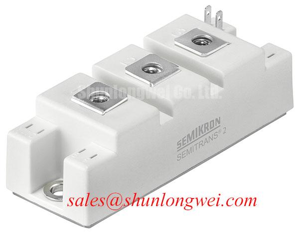
The Semikron SKM200GB063D is a high-current IGBT module specified for applications requiring a 600 V collector-emitter voltage and a 200 A continuous collector current under the stated case-temperature condition. Its electrical and thermal limits make it relevant for evaluation in industrial inverter stages, regenerative braking converters, commercial string inverters, and microgrid energy-storage power conversion, subject to complete system verification.
| Parameter | Official Specification | Conditions |
| Collector-emitter voltage, VCES | 600 V | Tj = 25°C |
| Continuous collector current, IC | 200 A | Tc = 80°C |
| Collector-emitter saturation voltage, VCE(sat) | 2.4 V typical | IC = 200 A, VGE = 15 V, Tj = 125°C |
| Gate-emitter voltage, VGES | ±20 V | Official device rating |
| Junction-to-case thermal resistance, Rth(j-c) | 0.14 K/W per IGBT | Official device rating |
| Junction-to-case thermal resistance, Rth(j-c)D | 0.3 K/W per diode | Official device rating |
| Total power dissipation, Ptot | 875 W | Tc = 25°C |
| Maximum junction temperature, Tjmax | 150°C | Official device rating |
The listed values are device specifications, not a complete converter operating prescription. Actual current, switching frequency, gate-drive conditions, coolant or heatsink performance, bus voltage, pulse duration, and ambient temperature determine whether the module remains inside its safe operating area. The system integrator should confirm the original Semikron documentation and the equipment manufacturer’s electrical and mechanical requirements before replacement.
💡 Bench Tip: Use ESD protection, keep the module at a documented cold condition, and compare diode polarity, gate-to-emitter isolation, and terminal resistance with a known-good unit before connecting the driver board.
Thermal troubleshooting should begin with the complete loss path rather than the module alone. The official Rth(j-c) of 0.14 K/W per IGBT and 0.3 K/W per diode describe the junction-to-case portion of the thermal path. They do not include interface resistance, heatsink resistance, airflow, coolant performance, mounting pressure, or enclosure temperature. The specified 875 W total power dissipation at Tc = 25°C also depends on its stated case-temperature condition and should not be treated as an unrestricted field dissipation value.
As an engineering calculation, multiplying the IGBT junction-to-case resistance by the listed total power dissipation gives a theoretical junction-to-case temperature rise of approximately 122.5 K if the entire dissipation were assigned to one IGBT and the conditions remained ideal. This calculation is a boundary illustration, not a permitted operating point. A real switching waveform contains conduction loss, turn-on loss, turn-off loss, diode recovery effects, and transient thermal behavior. A transient peak-junction estimate therefore requires the manufacturer’s thermal impedance curve and the measured pulse profile.
For heavy pulsed overloads, capture collector-emitter voltage, collector current, gate-emitter voltage, and case temperature in the same test sequence. A fault that appears only during turn-off may involve stray inductance or an unsuitable gate loop, while a fault that develops during sustained current may involve thermal interface quality or heatsink capacity. Verify the peak switching voltage against the 600 V VCES rating under the actual bus and commutation conditions. Minimize the high-current commutation loop and place the gate-drive return path according to the module and driver layout requirements; the final clearance and inductance targets must be determined by the system engineer through switching tests.
Multi-R thermal models are useful when the load contains repeated overload pulses, but they should not be populated with guessed time constants. Use the appropriate Semikron transient thermal data where available, separate the IGBT and diode heat sources, and account for the thermal recovery between pulses. If the source data is unavailable, report the result as an Engineering Recommendation to obtain validated thermal impedance information rather than presenting a calculated peak junction temperature as a guaranteed value.
In a commercial string inverter or microgrid storage converter, regenerative current can raise switching and conduction losses during battery charging or DC-link energy recovery. A braking chopper may also route energy into a high-power resistor, producing a short-duration thermal event that is different from normal inverter loading. The resistor, chopper duty cycle, DC-link control, and enclosure cooling must be evaluated together. The SKM200GB063D rating alone does not establish the allowable braking-energy profile.
SKM200GB063D Thermal-Electrical Optimization: Multi-Module Parallel Current Sharing Practical Tuning
When several IGBT modules are considered for a parallel phase leg, static and dynamic current sharing require separate checks. A positive temperature coefficient of VCE(sat) can support a stabilizing tendency during steady-state operation, but the effect must be confirmed from the relevant output characteristics at the intended gate voltage, current, and junction temperature. The typical 2.4 V VCE(sat) value is specified at IC = 200 A, VGE = 15 V, and Tj = 125°C; it is not a universal value for every load or switching condition.
Match the electrical path from the DC bus to each module as closely as the mechanical architecture permits. Equal-length power connections, comparable contact resistance, and symmetrical gate-loop geometry help reduce dynamic imbalance. The driver should be checked for propagation delay, gate resistance, negative transients, and common-emitter voltage movement. If the module’s exact terminal arrangement or internal connection drawing is required, use the original Semikron mechanical and electrical documentation rather than assuming that a visually similar module has the same pin relationship.
Desaturation protection is a system-level response to abnormal collector-emitter voltage during commanded conduction. It should be coordinated with gate-drive blanking, fault qualification, controlled turn-off, and DC-link discharge behavior. A protection design may specify a response objective below 3 μs as a Typical Starting Point for bench evaluation, but the appropriate timing is determined by the driver, noise environment, short-circuit withstand characteristics, and validated protection test. This timing is not an official SKM200GB063D rating supplied in the stated parameter set.
A two-stage soft turn-off sequence can be evaluated as an Engineering Recommendation: first limit the gate-drive energy quickly enough to interrupt the fault, then control the remaining current transition to reduce collector-emitter overshoot. The gate clamp, isolation barrier, fault latch, and driver supply must be tested as one protection chain. Observe the turn-off waveform at the module terminals with suitable measurement bandwidth and probe technique. An apparently late fault signal may be caused by sensing placement, propagation delay, or common-mode interference, so it should not be assigned to the IGBT without waveform evidence.
Dead-time and non-overlap settings also influence parallel current sharing and bridge safety. Excessive dead-time can increase diode conduction and recovery stress, while insufficient dead-time can create cross-conduction. Designers should verify the selected interval during high-side and low-side gate measurements, and the general principle of non-overlapping bridge control is described in Dead-Time Insertion and Non-Overlap Gate Driving in H-Bridges. Gate-emitter voltage must remain within the official ±20 V VGES rating, including switching transients and driver faults.
For a lower-current comparison within the same broad product family, engineers may review SKM100GB063D. This is a neutral cross-reference for electrical and mechanical evaluation, not a prescriptive substitute. The original bus voltage, current profile, gate-drive interface, thermal path, and mounting arrangement must all be checked before any cross-model decision.
Benchtop Waveform Tuning: Mitigating Stress via Atmospheric Neutron Radiation Impact on SKM200GB063D
Altitude and atmospheric radiation require disciplined qualification language. The supplied product data confirms a 600 V VCES rating, but it does not provide a product-specific neutron-induced Single Event Burnout curve, FIT rate, altitude derating factor, or operating-life prediction. A numerical SEB failure rate cannot be calculated responsibly from the electrical ratings alone. Any claim involving terrestrial neutron flux, failure probability, or a twelve-device assembly would require authoritative test data, defined geographic exposure, bias conditions, shielding, mission profile, and statistical methodology.
For equipment installed above approximately 2000 m, treat the altitude question as a Design Consideration rather than an automatic derating rule. Review the converter manufacturer’s insulation coordination, creepage and clearance requirements, cooling derating, enclosure pressure, and environmental qualification. The system designer should verify DC-link peak voltage, switching overshoot, repetitive avalanche exposure, and transient protection at the actual installation altitude. The 600 V rating is an absolute device boundary under its specified conditions, not a guarantee that every high-altitude topology remains adequately protected.
On the bench, start with a low-energy switching test and confirm the probe reference, gate waveform, current rise, turn-off overshoot, and diode commutation behavior. Increase operating stress only under a documented test plan with current limiting and fault shutdown. If a waveform changes with probe placement, cable routing, or isolation configuration, investigate measurement common-mode coupling before attributing the result to device degradation. Industrial inverter control boards using optocouplers or digital isolators should also be checked for common-mode transient immunity under the measured switching edge; the component’s presence does not independently establish compliance with a complete CISPR or EN 55011 installation.
Gate-oxide reliability is another reason to monitor the actual gate waveform instead of relying only on the driver supply label. Repetitive positive or negative excursions outside the normal control range can contribute to dielectric stress. The general mechanism of time-dependent dielectric breakdown is discussed in Time-Dependent Dielectric Breakdown of Gate Oxides. That industry principle should not be converted into a model-specific lifetime claim without Semikron qualification data.
For field troubleshooting, compare a suspect phase leg with a known-good phase under the same bus voltage and load command. Check whether the abnormality follows the module, remains with the driver channel, or changes with the power connection. Record the cold-state gate-to-emitter condition, diode polarity, terminal resistance, and insulation test result using the equipment manufacturer’s approved procedure. The Field Engineer’s Handbook can be used as a practical reference for structured testing and failure analysis.
Assembly Integrity & Layout Architecture: Implementing Baseplate Thermal Grease Layer Control for SKM200GB063D
Thermal installation begins with mechanical inspection. Clean the heatsink contact area, check for burrs or contamination, and inspect the module baseplate for visible distortion before applying thermal interface material. The supplied data does not state a module outline, baseplate flatness tolerance, fastener type, or manufacturer mounting torque. Those values must come from the applicable Semikron mechanical drawing and the equipment assembly specification.
A thin, continuous thermal compound layer is a Design Consideration for reducing air gaps between the baseplate and heatsink. A controlled starting range of 50 to 100 μm may be used only as an Engineering Recommendation when the compound manufacturer and mechanical drawing support it; it is not an official SKM200GB063D parameter. Excess compound can increase contamination risk and mechanical spread, while insufficient compound can leave dry areas. Apply enough material to fill surface irregularities, then verify coverage after a controlled trial installation.
Baseplate curvature compensation should be handled through the specified mounting sequence rather than by forcing the module flat with excessive fastener load. Use the prescribed cross-pattern or staged sequence, keep the heatsink supported, and confirm that the pressure is distributed across the mounting surface. If a disc-spring or flat-press clamping arrangement is used, calibrate spring height or clamping force against the mechanical drawing and inspect the springs for loss of elasticity. Do not infer the required force from the 0.14 K/W or 0.3 K/W thermal resistance values; thermal resistance and mechanical load are separate specifications.
Double-sided cooling or a two-surface thermal architecture demands independent verification of both interfaces. Check that the secondary heatsink does not introduce bending, terminal strain, or unequal pressure. After assembly, measure case temperature at comparable operating points and compare the IGBT and diode conduction paths separately. A rising case temperature with normal electrical waveforms may warrant interface inspection, while uneven phase temperatures may require review of current sharing, bus geometry, and driver timing.
Keep the power commutation loop compact and separate high-current switching paths from sensitive gate and fault-sense wiring. The isolation barrier, optocoupler or digital-isolator return path, and desaturation sensing loop should be routed to limit capacitive coupling during high dv/dt events. Final clearance, creepage, gate resistance, dead-time, and protection thresholds are system-determined values that require validation with the assembled heatsink, busbar, driver, and enclosure.
Before energizing the repaired assembly, verify fastener seating, thermal compound spread, gate polarity, diode direction, DC-link polarity, and isolation according to the approved service procedure. Confirm that the gate driver remains within the official ±20 V VGES limit during startup and switching. Only after these static checks should the converter proceed to controlled low-power waveform testing.