



Content last revised on September 23, 2026
Benchtop Waveform Tuning: Mitigating Stress via Junction to Case Thermal Network Simulation on FS100R12KT4G_B11
Before fitting the FS100R12KT4G_B11, isolate the converter, inspect the EconoPACK™ 3 contact area for mechanical damage or contamination, and verify that the original gate-board terminal mapping matches the removed module.
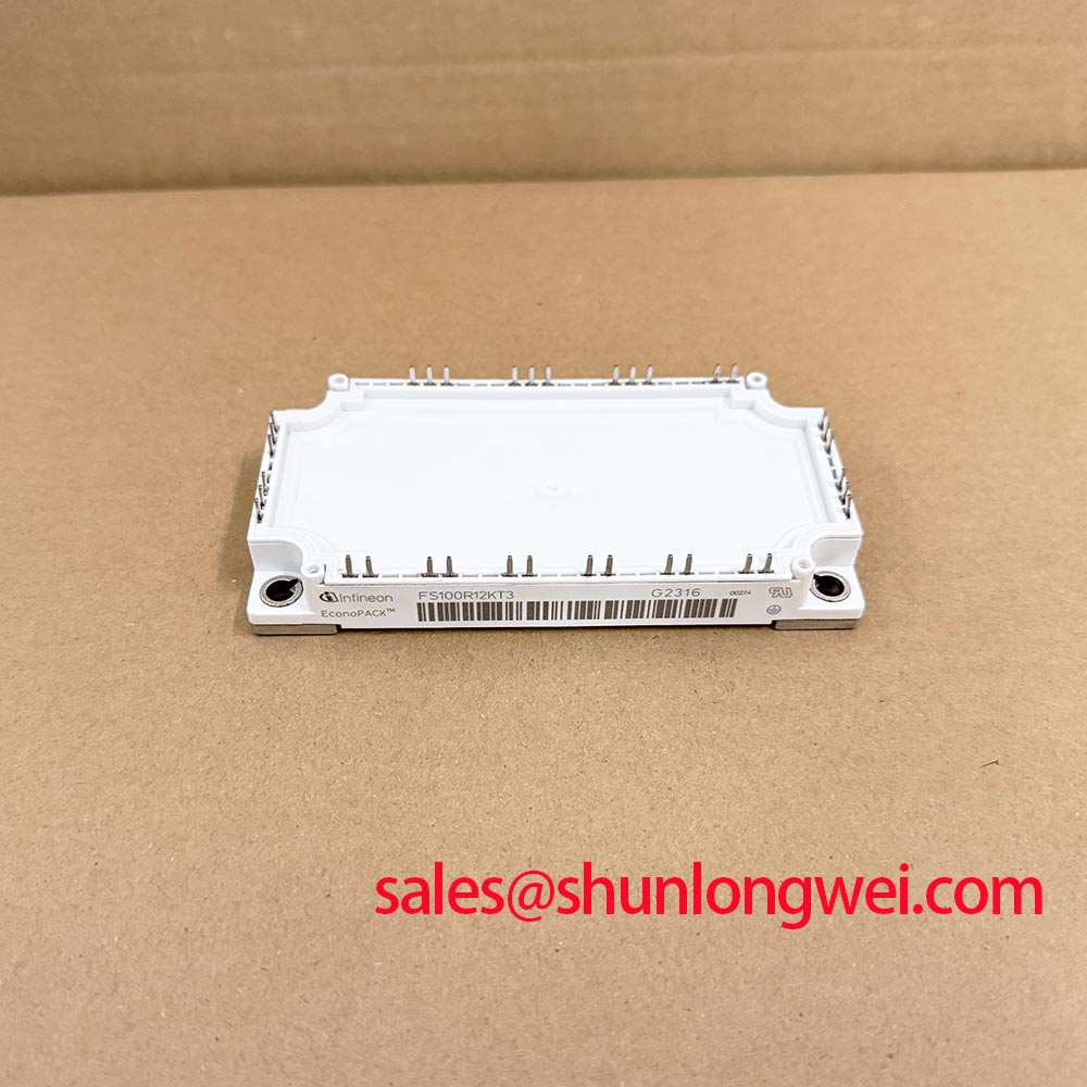
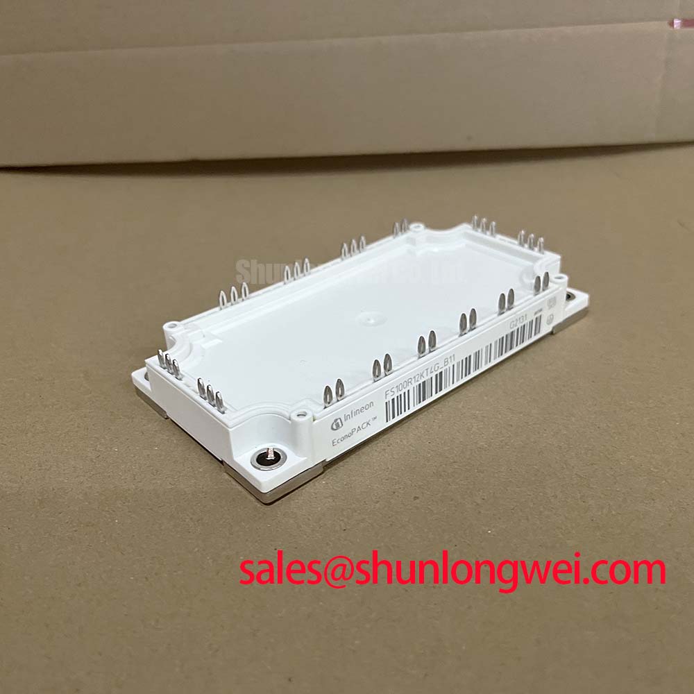
The Infineon FS100R12KT4G_B11 is a 1200 V, 100 A four-pack IGBT module configured as an H-bridge. Its stated current rating applies at Tc = 100°C, while the official maximum junction temperature is 175°C. The module uses TRENCHSTOP™ IGBT4 technology and an EconoPACK™ 3 package with PressFIT pins.
| Official Specification | Value |
|---|---|
| Manufacturer | Infineon |
| Collector Emitter Voltage, VCES | 1200 V |
| Continuous Collector Current, IC at Tc = 100°C | 100 A |
| Power Topology | Four Pack H Bridge |
| IGBT Technology | TRENCHSTOP™ IGBT4 |
| Package | EconoPACK™ 3 with PressFIT pins |
| Maximum Junction Temperature, Tvj max | 175°C |
These ratings are Official Datasheet Specifications and define the electrical and thermal identity of the module. They should not be treated as automatic permission to operate a complete inverter at those limits. DC link voltage variation, commutation inductance, switching frequency, heatsink capability, pulse duty, gate-drive behavior, and protection response all determine the actual operating boundary.
For a replacement or a new inverter assembly, begin with a controlled waveform review rather than assuming that a 100 A module will reproduce the behavior of the prior power stage without adjustment. The FS100R12KT4G_B11 has a 175°C maximum junction-temperature rating, but junction temperature is not directly visible at the module surface during a switching event. A thermal model helps relate measured loading to the thermal path between silicon junction, module case, thermal interface, and heatsink.
Engineering Calculation can be used when the original Infineon transient thermal impedance data and the actual switching-loss estimate are available. The temperature rise during a pulse is determined by the loss energy applied over time and the appropriate junction-to-case transient thermal impedance at that pulse duration. Repetitive pulse loading requires the thermal response of earlier pulses to be included rather than assessed as isolated events. This approach is especially relevant when inverter welders or medium-frequency induction heating supplies repeatedly move between low-load and high-current operating states.
During bench commissioning, measure collector-emitter voltage and collector current with probe connections arranged to minimize added loop area. Compare the turn-on and turn-off waveform shape with the known system behavior where available. A rising case temperature, a changing switching waveform, or a gate signal that loses its intended amplitude can each contribute to a reduced thermal margin. None of these observations alone identifies a single root cause, so the gate drive, DC link, cooling surface, controller timing, and load condition should be examined together.
Design Consideration: use the original thermal data and the actual mounting stack when estimating junction temperature. A heatsink that appears adequate at steady load may behave differently during clustered energy pulses, especially where airflow, thermal interface condition, or enclosure temperature has changed since the equipment was first commissioned.
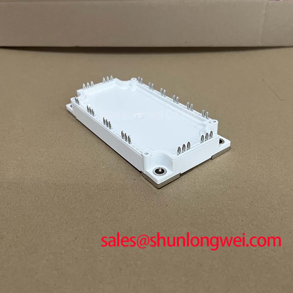
The EconoPACK™ 3 PressFIT interface deserves particular attention during replacement work. The board must be supported so insertion force is not transferred into adjacent traces or connector regions. Check for board bowing, incomplete engagement, and signs that the module does not sit parallel to its intended mounting plane. Mechanical distortion can create intermittent electrical contact or uneven thermal contact that becomes visible only after the converter warms.
🔧 Bench Diagnostic: Disconnect and discharge the DC link before connecting or removing oscilloscope probes, gate-drive leads, or load cables around the power stage.
For systems that need a same-class comparison during documentation review, the linked FS100R12N2T4 can be examined as a separate reference part. Its suitability is system-determined and requires confirmation of topology, package interface, drive conditions, protection behavior, and the original equipment documentation.
Assembly Integrity and Layout Architecture: Controlling Turn Off di dt Induced Peak Voltage
The 1200 V VCES rating establishes the official blocking-voltage boundary for the FS100R12KT4G_B11. Actual turn-off voltage is influenced by DC link voltage plus the inductive component associated with the current-change rate and the commutation-loop inductance. In practical terms, a fast current interruption through a loop with stray inductance creates an added voltage excursion. The relevant peak must therefore be verified at the module terminals under representative switching conditions, not inferred from nominal bus voltage alone.
Design Consideration: minimize the physical area of the commutation path between the DC link capacitor, module terminals, and return conductors. Close-coupled, symmetrical conductor geometry can reduce parasitic inductance and helps suppress turn-off overshoot. The final layout must be validated through switching tests that confirm peak voltage margin against the DC-link condition, load current, gate-drive behavior, and operating temperature used by the equipment.
When a snubber network is present, preserve its original electrical placement and inspect it as part of the assembly rather than treating it as an unrelated accessory. A capacitor or resistor network positioned remotely from the commutation loop can have a different effect from the intended local suppression network. System engineers should verify the component condition, connection resistance, and waveform result after any power-stage repair.
Where multiple power modules are used in parallel, static sharing and dynamic sharing are different checks. The positive temperature characteristic associated with IGBT conduction behavior can assist static current balance under appropriate conditions, but it does not remove the need for matched conductor geometry and symmetrical gate-drive paths. Unequal path resistance, unequal loop inductance, or different drive timing can cause current imbalance during transitions even when the modules appear similar in a static measurement.
The four-pack H-bridge arrangement can simplify a converter power stage, yet each switching cell must still be considered as part of its full commutation loop. For industrial inverter welder and induction-heating equipment, review the DC-link capacitor location, busbar layers, gate-board attachment, current sensing path, and the physical return route together. A local waveform anomaly may originate in any of these connected sections.
In equipment that includes a separate input rectifier or complementary power section, the BSM100GAL100D is a relevant linked device for topology documentation. It is not an asserted replacement for this H-bridge module. Engineers should compare the actual circuit role, voltage class, package arrangement, cooling interface, and control method before making a sourcing or repair decision.
Field Diagnostics and Commissioning: Output Sinusoidal Filter Versus dv dt Reactor in FS100R12KT4G_B11 Topologies
At commissioning, test the power stage first with the intended load path and cable arrangement, because output wiring can influence the waveform seen beyond the inverter terminals. Long motor leads and poorly matched cable or load impedances can produce reflected voltage behavior. Depending on the cable, termination, motor condition, and switching edge, the remote terminal waveform can differ substantially from the waveform measured at the module.
A dv dt reactor and a sinusoidal output filter address different integration objectives. A reactor can moderate output edge behavior, while a sinusoidal filter is evaluated where the system requires a waveform closer to a sinusoidal load voltage. Neither should be selected by a generic rule. The load type, cable route, switching strategy, allowable voltage stress, thermal behavior, acoustic constraints, and control-loop requirements need to be assessed at system level.
For an industrial inverter welder, measure output behavior under the actual welding sequence rather than only at idle. Arc establishment, current regulation response, and output-cable placement can change stress conditions from those seen in an unloaded test. For a medium-frequency induction heating supply, evaluate the resonant load arrangement, work-coil connection, and controller protection response during the intended heat cycle. The module’s official 1200 V and 100 A at Tc = 100°C specifications remain fixed, while the application waveform determines the operating stress imposed around those ratings.
Field diagnostics should use evidence from several measurements. An overvoltage event may be associated with output-cable reflections, DC-link disturbance, gate-drive instability, unsuitable probing technique, a damaged suppression network, or load-side behavior. Verify the measurement setup against a known-good signal path where possible, then compare voltage, current, gate command, and fault timing. This avoids assigning a single cause to a waveform before the entire switching loop has been checked.
Where a filter is being considered after a repair, maintain appropriate electrical separation and inspect routing between high-energy conductors, low-level control lines, and sensing connections. Design Consideration: physical segregation and controlled return paths help reduce unwanted coupling, but clearances, insulation coordination, and final compliance obligations are determined by the complete equipment design rather than by the IGBT module alone.
Current-generation power-semiconductor developments can provide useful context for switching and thermal design practices. The external discussion of Infineon TRENCHSTOP™ IGBT technology developments concerns a later technology generation and should not be used to replace the official specifications of this IGBT4 module. For the FS100R12KT4G_B11, evaluate only the confirmed ratings and the measured behavior of the installed system.
FS100R12KT4G_B11 Thermal Electrical Optimization: Gate Drive Loop Geometry for Practical Tuning
The gate-drive loop should be treated as a measurement-sensitive control path, not as an extension of the main power bus. Fast collector current transitions can induce voltage in shared emitter or return conductors. If the gate reference shares too much of the high-current return path, that induced voltage can alter the effective gate-emitter command and contribute to oscillation, delayed turn-off, or inconsistent switching behavior.
Engineering Recommendation: keep gate-drive routing compact and separate the gate return from the main high-current emitter path wherever the module terminal arrangement and original drive-board design support an auxiliary return connection. The system integrator should verify the exact terminal assignment from the original module documentation and gate-board schematic. Do not assume an auxiliary terminal exists or has a particular function from package appearance alone.
Gate resistance, drive voltage, desaturation protection, soft shutdown behavior, and controller dead time are system-level variables. They should be retained from the established converter design unless waveform testing demonstrates a need for controlled adjustment. A faster transition can reduce one loss mechanism while increasing voltage overshoot or electromagnetic coupling. A slower transition can reduce edge stress while increasing switching energy. Practical tuning is the verified balance of these effects under the actual DC link, load, temperature, and protection conditions.
Use a differential voltage probe and an appropriately referenced current measurement to observe switching events at the intended operating point. Then review gate waveforms at the module-side connection, not solely at the controller output. A clean controller command does not prove that the command remains clean at the module terminals after interaction with the power loop. Check for ringing, unexpected gate displacement, timing asymmetry between bridge devices, and changes as temperature rises.
For demanding thermal-margin assessment, the mounting interface, heatsink flatness, airflow condition, and control protection should be reviewed alongside gate-loop geometry. The 175°C maximum junction-temperature specification is an official limit, while the usable operating margin is established through application-specific testing. The practical thermal principles discussed in The Advanced Thermal Management Revolution can support a broader review of heat-flow paths when assessing a repaired or newly integrated power assembly.