Content last revised on September 15, 2026
Field Diagnostics & Commissioning: Semiconductor Protection Fuse Selection in T508N16 Topologies
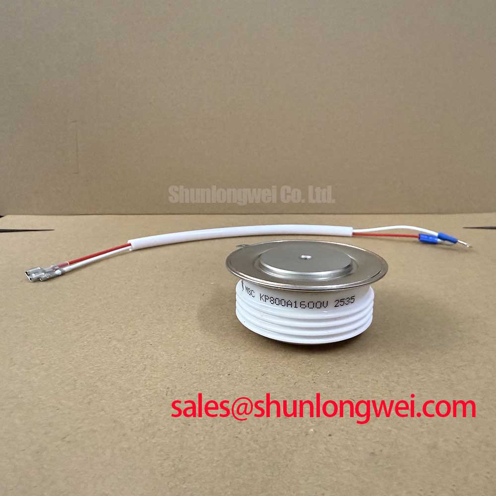
Before fitting a replacement device, isolate the converter, remove pressure from the clamping stack, and compare the cold-state anode, cathode, and gate terminal relationships against the original circuit documentation. T508N16 is an Infineon capsule thyristor rated at VDRM/VRRM 1600 V, ITAVM 508 A at Tc = 85 °C, and a specified ITRMS rating of 800 A, with a maximum junction temperature of 125 °C. These are Official Datasheet Specifications and define key electrical limits that must be retained when evaluating a replacement in a high-current controlled rectifier.
Use the meter diode range only as a comparative screening method with the unit fully disconnected from surrounding circuitry. A gate-to-cathode reading that differs materially from a known-good device, or unexpected conduction between anode and cathode without a valid triggering arrangement, calls for additional controlled bench evaluation. The meter reading itself is not a switching-performance qualification and should not be treated as proof of dynamic suitability.
💡 Bench Tip: Use ESD precautions, document the terminal orientation before disassembly, and compare cold-state readings with a known-good unit tested using the same meter and leads.
Semiconductor fuse selection is a Design Consideration, not an inherent rating of the T508N16. During a dead-short investigation, the repair team should obtain the fuse manufacturer’s total clearing I²t curve and compare it with the converter protection study, the transformer fault capability, conductor limits, and the applicable thyristor surge-withstand information from the original equipment documentation. The goal is coordinated interruption before fault energy damages adjacent buswork, heat sinks, clamp hardware, or parallel devices. The supplied T508N16 ratings establish continuous current capability, but they do not replace a system-level I²t coordination record.
Check that the fuse body, holder contacts, and busbar interfaces show consistent contact pressure and no heat discolouration. A high-resistance fuse interface can create a local thermal problem while the device itself remains within its specified average-current rating. Where a repair assessment identifies a lower-current press-pack candidate such as TD210N12, engineers should compare blocking-voltage class, average and RMS current requirements, clamping geometry, gate connection arrangement, cooling conditions, and all original converter requirements before deciding whether it is electrically and mechanically appropriate.
| Official Specification | T508N16 Value | Commissioning Relevance |
|---|---|---|
| Repetitive peak off-state and reverse voltage | 1600 V | Verify against measured transient peaks and the original line-side protection arrangement. |
| Average on-state current | 508 A at Tc = 85 °C | Compare with the actual thermal boundary used by the converter manufacturer. |
| RMS current | Specified rating: 800 A | Review against waveform current, transformer loading, and fault-path capability. |
| Maximum junction temperature | 125 °C | Use as the device temperature limit during thermal verification. |
| Package | Disc / Capsule | Requires a correctly aligned pressure-contact clamping assembly. |
T508N16 Operational Boundaries: Evaluating AC Line Surge Immunity, Lightning Transient Limits
Measure the incoming line arrangement and inspect the existing surge-protection path before attributing a failed thyristor to an AC transient. The 1600 V VDRM/VRRM rating is an Official Datasheet Specification for repetitive off-state and reverse voltage; it is not a statement that the installed converter is immune to arbitrary lightning or switching surges. Surge behavior depends on the supply network, transformer leakage inductance, protective-device coordination, cable routing, grounding, and the actual waveform at the device terminals.
For an induction melting or hardening furnace supply, the line-side protection review should include the condition and placement of metal-oxide varistors, suppression capacitors, surge arresters where fitted, RC networks, and earth-bonding connections. IEC 61000-4-5 is commonly used as a system-level surge test reference. Design Consideration: the system engineer should compare the specified test environment and measured clamp response with the rectifier’s voltage margin rather than assigning compliance or immunity to the T508N16 alone.
Inspect MOV assemblies for cracked housings, heat marks, loose terminals, or evidence that their thermal disconnect function has operated. An MOV can become electrically altered after repeated stress, while a visually sound part may still require measured verification. RC snubbers placed ahead of or across controlled rectifier sections should be checked for capacitor degradation, resistor overheating, and short lead routing. Their effectiveness is determined by the actual inductive path and converter commutation waveform, so values should remain governed by the original equipment design or validated bench testing.
The pressure-contact package supports a clamped thermal path, but clamping force and contact-plane condition belong to the equipment assembly specification. Do not infer a mounting torque from unrelated semiconductor housings. ⚠️ Field Alert: Never energize a press-pack thyristor stack after reassembly unless the specified clamp hardware, alignment procedure, and pressure requirements have been verified against the original equipment documentation.
Some high-temperature packaging discussions refer to eutectic materials or high-performance polymers; those materials must not be assumed to be inside this device. For general reference only, engineers reviewing thermal-packaging terminology can consult information on eutectic material systems and PEEK high-durability polymers. Neither reference establishes the internal construction or environmental qualification of T508N16.
Assembly Integrity & Layout Architecture: Implementing Harmonic Current Injection and Line Filter for T508N16
Confirm the anode-to-cathode orientation, gate lead routing, and busbar stack order before applying any firing signal. In line-commutated rectifier bridges, controlled firing angle changes the transfer of AC supply energy into the DC load. As the firing angle is delayed from the vicinity of 0 degrees toward 150 degrees, the converter generally transfers less useful rectified power and draws a waveform with increasing reactive and harmonic content. The exact current shape depends on source impedance, transformer design, DC reactor behavior, load condition, commutation overlap, and the selected rectifier topology.
This behavior matters when the T508N16 is assessed for medium-frequency induction melting and hardening furnace power equipment. The stated 508 A average current at Tc = 85 °C and specified 800 A RMS current rating should be checked against logged operating current at the real firing conditions, not only against a nominal furnace nameplate. A converter that appears acceptable during steady heating can experience materially different thermal loading during output adjustment, charge changes, or control recovery after an interruption.
Design Consideration: arrange the power loop to keep parallel current paths geometrically consistent and minimize parasitic inductance, particularly where line filters, commutation inductors, and suppression components connect to the controlled bridge. The technician should verify busbar flatness, insulation spacing, clamp alignment, and terminal cleanliness before evaluating control-board faults. A distorted line-current waveform can originate from more than one source, including timing asymmetry, supply imbalance, transformer condition, a degraded filter branch, unequal thyristor triggering, or load-side changes.
Where the original equipment includes line filtering or harmonic-control equipment, record its installed connections before removal. Replacing a thyristor while altering the filter return path, protective-earth connection, or busbar sequence can invalidate comparison with prior measurements. Engineers should use current probes and voltage probes rated for the actual installation to compare phase currents and device terminal waveforms against the approved converter service procedure.
For broader background on switching-device principles, junction limits, and power-semiconductor terminology, see The Ultimate IGBT Knowledge Base. The material is useful for foundational context, while T508N16 integration must remain governed by its own official ratings and the host converter documentation.
T508N16 Operational Boundaries: Evaluating RC Snubber Network Optimization to Prevent Limits
Begin an RC snubber review with the installed circuit rather than a generic resistor-capacitor value. The T508N16 is a thyristor, and unintended triggering risk is influenced by the device terminal voltage rate of change, gate circuit noise, common-mode coupling, wiring inductance, and the commutation conditions of the complete rectifier. The available Official Datasheet Specifications confirm the 1600 V blocking class, current ratings, 125 °C maximum junction temperature, and disc/capsule construction, but no unprovided dv/dt, di/dt, gate-trigger, snubber, or reactor value should be assumed for this exact part.
An Engineering Recommendation is to inspect the existing snubber capacitor for capacitance loss, leakage, physical damage, and secure connections, then examine the series resistor for resistance change and thermal evidence. A snubber branch that has been disconnected, rerouted, or fitted with unsuitable replacement parts may leave the thyristor exposed to a different commutation environment. Oscilloscope measurements should be made at the device terminals using an appropriate differential measurement method, with peak voltage checked against the DC-link and line-transient boundaries during representative switching tests.
A series saturable reactor, where present in the original topology, can influence current rise and commutation stress. Its suitability depends on the converter’s fault response, source inductance, load cycle, thermal design, and trigger timing. The system designer should validate the combined reactor, fuse, snubber, and gate-drive behavior after any service change rather than treating one component as an isolated cure.
Keep the gate connection separated from high-current power conductors wherever the original assembly permits, and inspect the return path for loose connections or contamination. Gate-cathode noise can be coupled from common-mode movement in the power circuit, particularly when a furnace supply changes operating state. If unexpected conduction remains under investigation, compare gate waveforms, phase voltages, and snubber-terminal voltage with a known-good signal path before replacing further hardware.
The T508N16 pressure-contact format should be evaluated as part of the complete thermal and electrical stack. Correct terminal polarity, consistent clamping, a verified protection path, and measured switching waveforms provide a sounder basis for return-to-service decisions than any assumed universal snubber setting.